Reducing plating stub reflections in a chip package using resistive coupling
一种芯片封装、电阻性的技术,应用在电路装置、电固体器件、含有印制电阻等方向,能够解决妨害封装体信号性能等问题
- Summary
- Abstract
- Description
- Claims
- Application Information
AI Technical Summary
Problems solved by technology
Method used
Image

Examples
Embodiment Construction
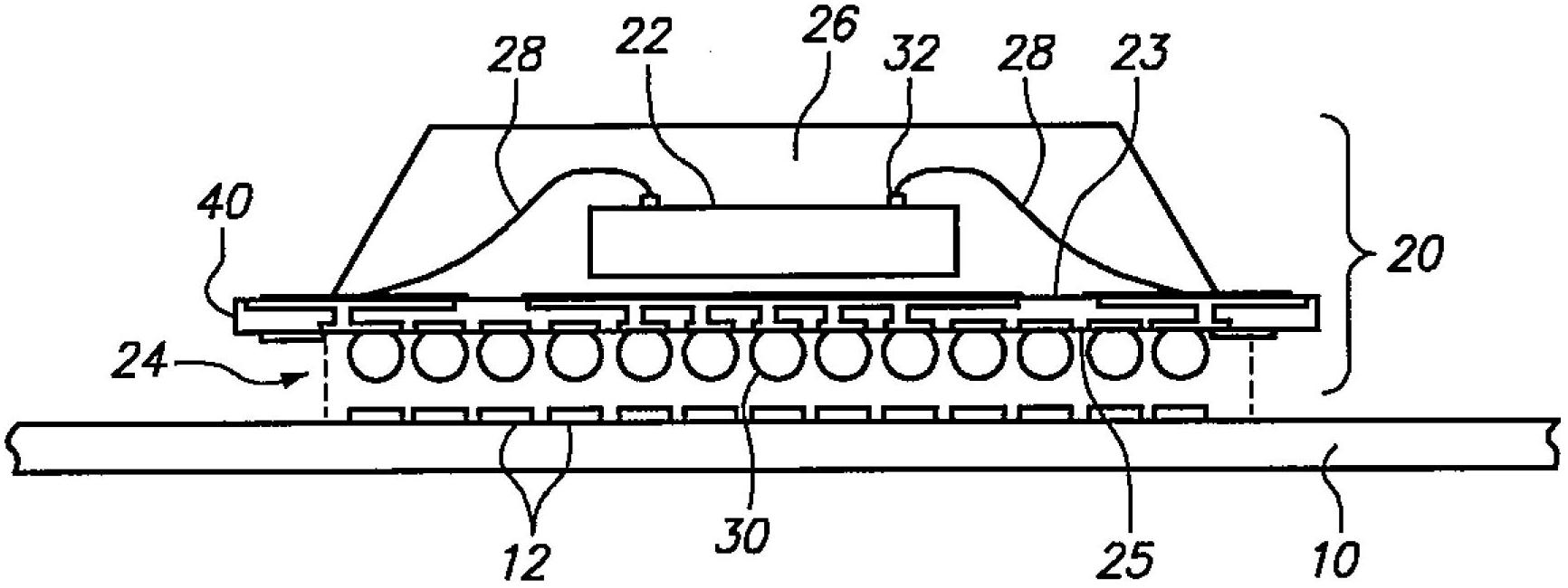
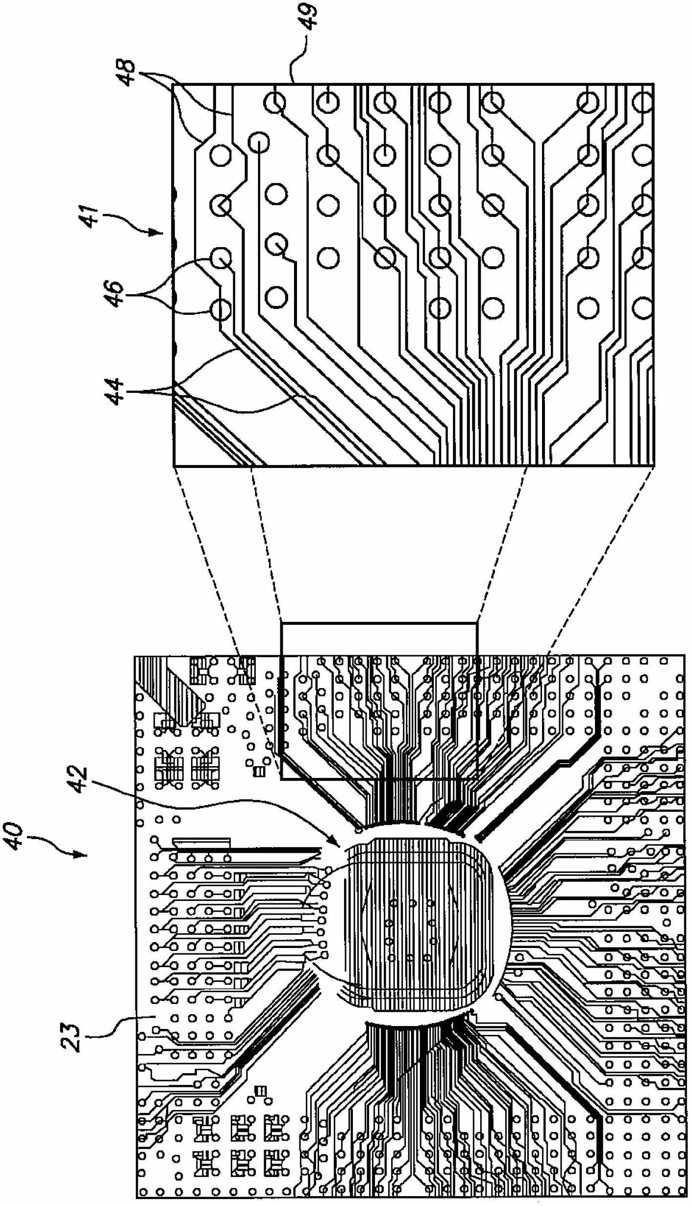
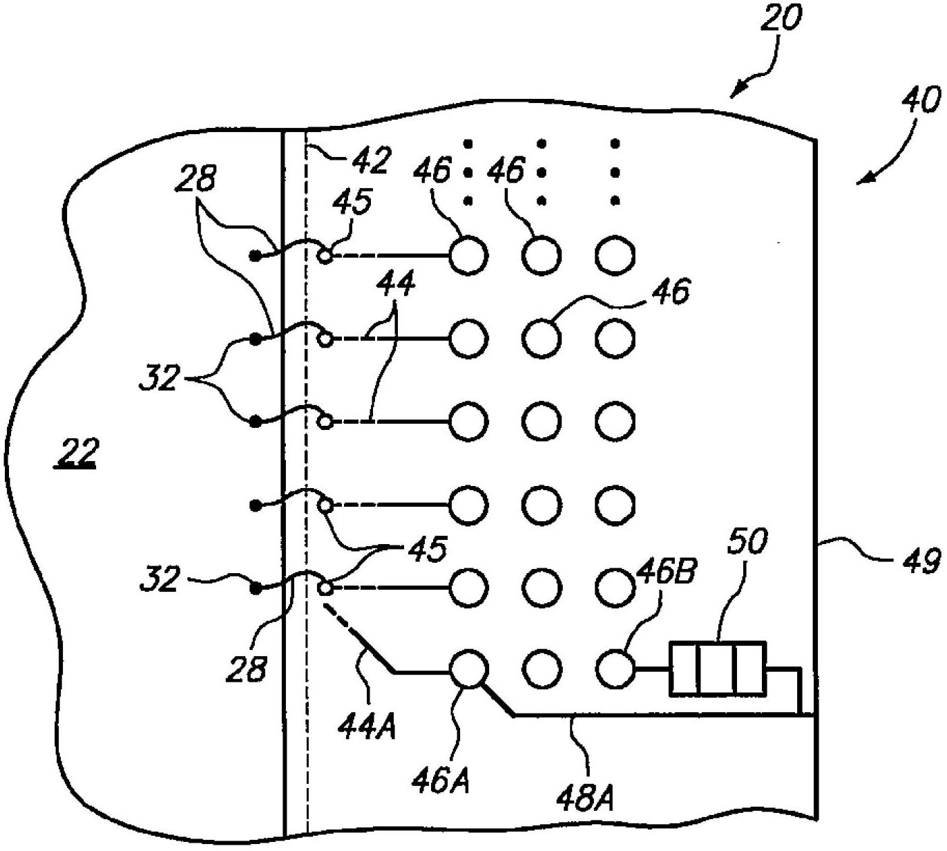
[0016] One embodiment of the present invention is a method of reducing resonant frequency in a high frequency chip package by utilizing a resistor to terminate a plating stub at an open end. The plating stub can be resistively coupled to ground using thin film resistors or discrete surface mount (SMT) resistors. Another embodiment of the present invention is a multilayer package substrate in a high frequency chip package, wherein the plating residue at the open end is resistively coupled to ground. Resistive coupling of plating strands to ground in accordance with the present invention provides an effective way of reducing the effects of plating strand reflections, and is more economical than other means of mitigating the effects of plating strands. The invention, in its various embodiments, is applicable to numerous chip package configurations known in the art. The principles of the invention discussed with respect to the illustrated embodiments are therefore also applicable...
PUM
 Abstract
Description
Claims
Application Information
 - R&D
- Intellectual Property
- Life Sciences
- Materials
- Tech Scout
- Unparalleled Data Quality
- Higher Quality Content
- 60% Fewer Hallucinations
Browse by: Latest US Patents, China's latest patents, Technical Efficacy Thesaurus, Application Domain, Technology Topic, Popular Technical Reports.
© 2025 PatSnap. All rights reserved.Legal|Privacy policy|Modern Slavery Act Transparency Statement|Sitemap|About US| Contact US: help@patsnap.com