
Wafer cleaning device and cleaning method

A technology for cleaning wafers and wafers, applied in cleaning methods and appliances, cleaning methods using liquids, chemical instruments and methods, etc., can solve problems such as difficulty in achieving uniformity of sound field intensity, low sound field intensity, and bubble rupture, and achieve improved Cleaning effect, satisfaction of uniformity, effect of eliminating damage

Inactive Publication Date: 2012-08-22
BEIJING SEVENSTAR ELECTRONICS CO LTD
View PDF8 Cites 14 Cited by
  • Summary
  • Abstract
  • Description
  • Claims
  • Application Information

AI Technical Summary

Problems solved by technology

However, due to the interference phenomenon of the megasonic sound field, many hot spots with high sound field intensity will be formed on the wafer surface, and many dead spots with low sound field intensity will be formed at the same time, and the uniformity of the sound field intensity on the wafer surface is difficult to achieve.
In addition, the hot spots formed by the megasonic sound field interference can easily cause the bubbles to burst, and the cavitation formed by the bubble bursts also increases the risk and possibility of damage to the microstructure of the graphics wafer
[0003] Although in the process of improvement, there is a method of using frequency scanning to reduce the formation of hot spots, but since the frequency scanning only surrounds this central frequency, and this scanning around the center frequency is only applied to one megasonic oscillator, the megasonic oscillator The natural frequency of the mechanical vibration is fixed (generally equal to the center frequency of the megasonic wave), and the change of the deviation from the center frequency will cause the amplitude of the vibrator to decrease and the energy of the transmitted megasonic wave to decrease, so that the acoustic energy density formed on the surface of the wafer increases with the Scanning frequency changes, unable to produce a uniform sound field
Although the method of frequency superposition and combination is also useful, since the voltage of frequency superposition combination is still applied to the same megasonic vibrator, the vibration of the vibrator is too large to affect the efficiency of electroacoustic conversion, which reduces the cleaning effect.

Method used


Image

  • Wafer cleaning device and cleaning method
  • Wafer cleaning device and cleaning method
  • Wafer cleaning device and cleaning method

Examples


Embodiment Construction

[0024] The specific implementation manners of the present invention will be further described in detail below in conjunction with the accompanying drawings and embodiments. The following examples are used to illustrate the present invention, but are not intended to limit the scope of the present invention.

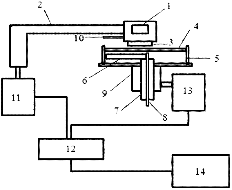
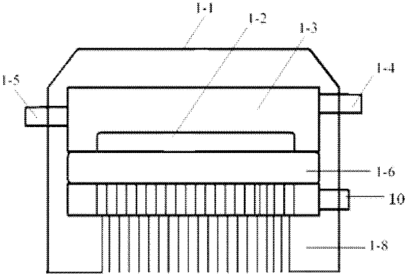
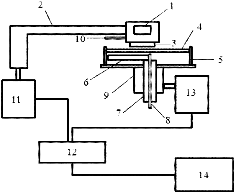
[0025] figure 1 It is a structural schematic diagram of a wafer cleaning device according to an embodiment of the present invention; refer to figure 1 , the device in this embodiment includes: a wafer carrying unit 5 for carrying a wafer 4, a wafer front megasonic cleaning nozzle 1 arranged above the wafer carrying unit 5, a wafer back megasonic cleaning nozzle 1 arranged in the wafer carrying unit 5. Acoustic wave cleaning unit 6, rotating shaft 9, hollow pipe 7, spray arm 2, spray arm motor 11, and wafer rotating motor 13, described wafer front megasonic wave cleaning nozzle 1 is provided with liquid inlet 10, and The side is provided with the liquid ejection outlet 3 ...


PUM


Abstract

The invention discloses a wafer cleaning device and a cleaning method and relates to the cleaning technical field of a semiconductor integrated circuit device. The wafer cleaning device comprises a wafer bearing unit for bearing a wafer, a wafer front surface ultrasonic cleaning nozzle arranged above the wafer bearing unit, a wafer back surface ultrasonic cleaning unit arranged in the wafer bearing unit, a rotary shaft, a hollow pipe, a spraying arm, a spraying arm motor and a wafer rotating motor. According to the invention, a uniform sound field is formed in cleaning fluid of the upper surface and the lower surface of the wafer through phase shift and distortion formed by the synthesis of ultrasonic wave with a first preset frequency, generated by the wafer front surface ultrasonic cleaning nozzle and ultrasonic wave with a second preset frequency, generated by the wafer back surface ultrasonic cleaning unit, so that the wafer is cleaned, the strength uniformity of the ultrasonic wave sound field on the wafer is met, the cleaning effect on the wafer is improved, meanwhile, the damage to the feature size and structure of the wafer caused by severe cavitation generated by the ultrasonic wave is reduced and eliminated.

Description

technical field [0001] The invention relates to the technical field of semiconductor integrated circuit device cleaning, in particular to a wafer cleaning device and a cleaning method. Background technique [0002] As the feature size of integrated circuits enters the deep sub-micron stage, the requirements for cleaning control in the wafer manufacturing process are getting higher and higher, and the uniformity of cleaning has become a challenging issue. Cleaning under the action of megasonic waves helps to improve the cleaning effect of the wafer, and can greatly improve the removal efficiency of polluting particles. However, due to the interference phenomenon of the megasonic sound field, many hot spots with high sound field intensity will be formed on the wafer surface, and many dead spots with low sound field intensity will be formed at the same time, so the uniformity of the sound field intensity on the wafer surface is difficult to achieve. In addition, the hot spots ...

Claims


Application Information

Patent Timeline
Patent Type & Authority Applications(China)
IPC IPC(8): B08B3/12B06B1/06H01L21/00
Inventor 刘伟吴仪张豹蔡家骏初国超
Owner BEIJING SEVENSTAR ELECTRONICS CO LTD
Learn More