Method and system for design rule checking of integrated circuit layout

A technology of integrated circuit and layout design, applied in computing, electrical digital data processing, special data processing applications, etc.

Active Publication Date: 2012-09-12
SHANGHAI FUDAN MICROELECTRONICS GROUP
View PDF1 Cites 36 Cited by
  • Summary
  • Abstract
  • Description
  • Claims
  • Application Information

AI Technical Summary

Problems solved by technology

Complex and diverse design rules pose challenges to traditional routing tools in terms of functionality and performance

Method used


Image

  • Method and system for design rule checking of integrated circuit layout
  • Method and system for design rule checking of integrated circuit layout
  • Method and system for design rule checking of integrated circuit layout

Examples


Embodiment Construction

[0030] Preferred embodiments of the present invention will be described in detail below in conjunction with the accompanying drawings.

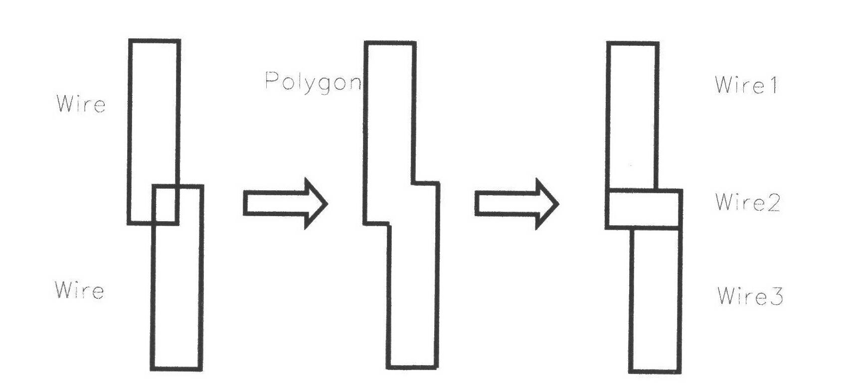
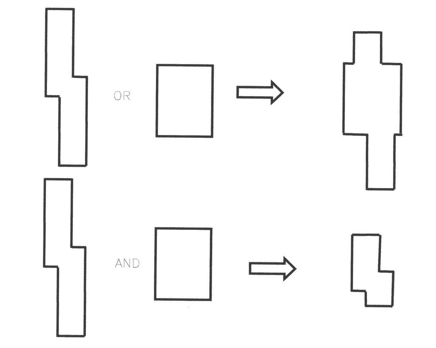
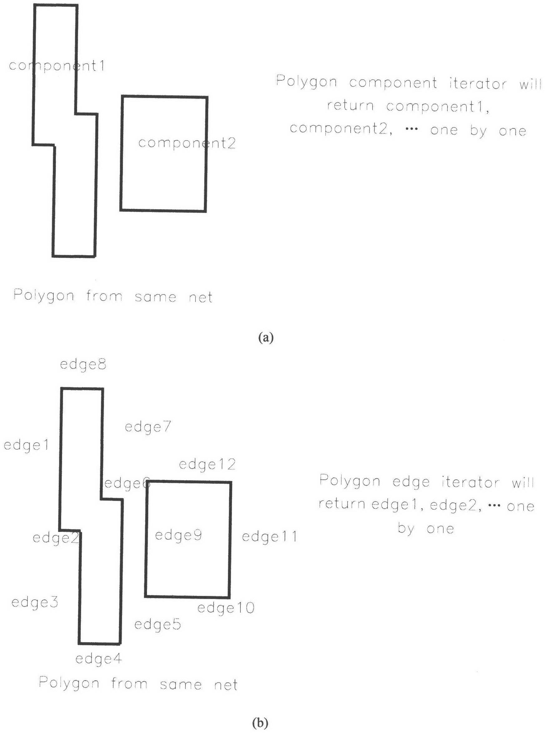
[0031] This embodiment designs a method for checking layout design rules of an integrated circuit based on polygon operations. For the input layout graph, this method abstracts it into a polygonal data representation defined by a series of horizontal boundaries, and provides an interface to convert between the rectangular traces generated by automatic routing and the layout polygons, such as figure 1 shown. At the same time, this method defines and implements the addition (UNION), subtraction (SUBSTRACT), and (AND) operation methods between polygons (see figure 2 ), and enumeration traversal operation methods for polygon connected regions and boundary edges, such as image 3 shown. On this basis, the routing tool can conveniently construct and delete layout polygons, and traverse polygon coverage rectangles and boundary edges according to...


PUM


Abstract

The invention discloses a method and a system for design rule checking of an integrated circuit layout. A layout graph is abstracted to be represented by polygon data defined by a series of horizontal borders, a polygon feature extraction method, a logical operation method among polygons and a method for enumeration and traverse operation of polygon connected regions and border edges are defined and achieved, and design rules are checked and marked on the basis. Data structure mutual transformation among interconnected rectangulars and layout polygons can be performed, the method for polygon operation and the enumeration and traverse operation of the polygon border edges is defined and achieved, and the design rules are checked on the basis. According to the method for the design rule checking of the integrated circuit layout, graph regions violating the design rules in the layout are also marked heuristically so as to enable local regions to be split and rerouted by automatic routing tools or designers to perform fine adjustment to the layout.

Description

technical field [0001] The invention belongs to the field of integrated circuit design, in particular to the technical category of integrated circuit design optimization under the integrated circuit manufacturing process with the line width of the interconnection line at or below 65nm. Background technique [0002] The integrated circuit is designed by the designer with the help of electronic design automation (EDA) tools to design the integrated circuit layout, delivered to the integrated circuit manufacturer, through the circuit mask preparation (Mask), and the wafer (Wafer) for oxidation, doping, photolithography A series of manufacturing processes such as transferring the circuit mask to the wafer, so as to realize its circuit function. The photolithography process in the manufacture of integrated circuits refers to the process of copying the mask pattern on the photoresist on the surface of the semiconductor silicon wafer to form a photolithographic image when using a m...

Claims


Application Information

Patent Timeline
Patent Type & Authority Applications(China)
IPC IPC(8): G06F17/50
Inventor 李卓远陈刚
Owner SHANGHAI FUDAN MICROELECTRONICS GROUP
Why Eureka
Try Eureka