High-precision band-gap reference circuit

A reference circuit, high-precision technology, used in regulating electrical variables, control/regulating systems, instruments, etc.

Inactive Publication Date: 2012-09-19
TIANJIN UNIV
View PDF4 Cites 2 Cited by
  • Summary
  • Abstract
  • Description
  • Claims
  • Application Information

AI Technical Summary

Problems solved by technology

[0003] However, when the paired MOS tubes in the circuit are not well matched, an offset volt

Method used


Image

  • High-precision band-gap reference circuit
  • High-precision band-gap reference circuit
  • High-precision band-gap reference circuit

Examples


Embodiment Construction

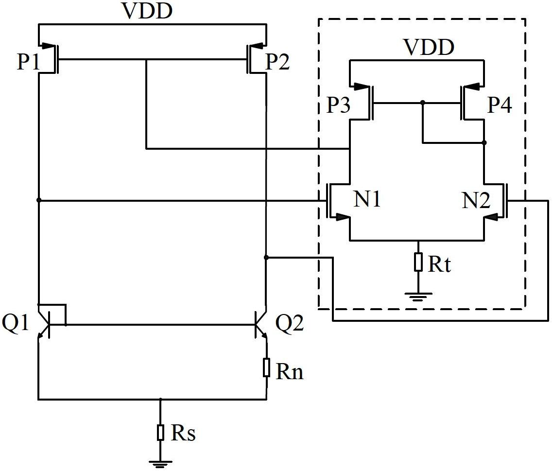
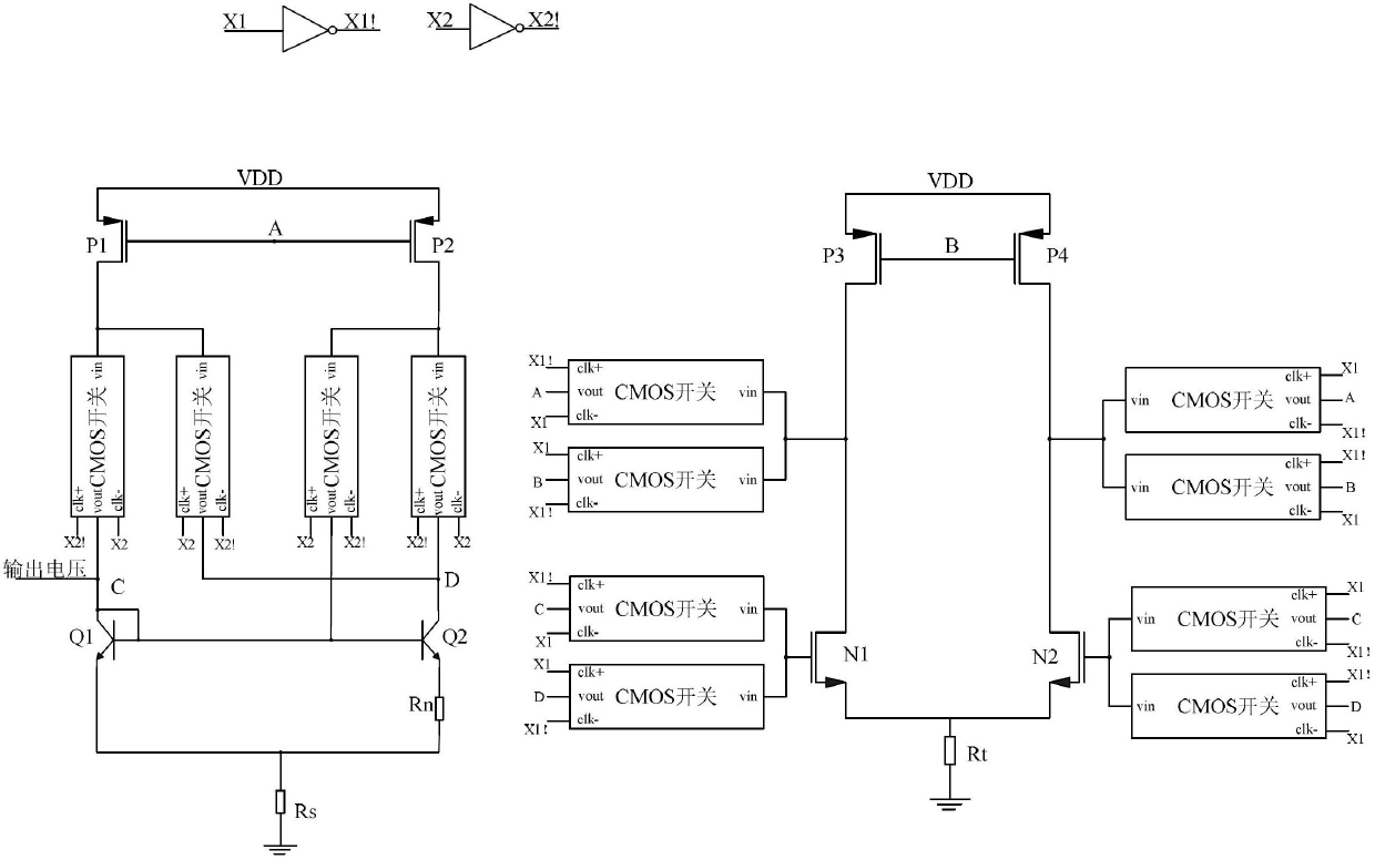
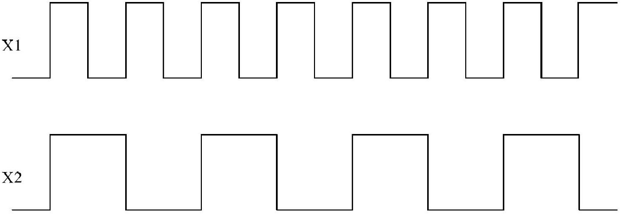
[0018] figure 2 It is the optimized bandgap reference circuit structure. Among them, X1 and X2 are divided by two clocks, and their waveforms are as follows image 3 As shown, the X1 cycle is 1us, and the X2 cycle is 2us. Figure 4 For the internal structure of the CMOS switch. Figure 5 The circuit structure of the inverter.

[0019] so by figure 2 It can be seen that during the periodic change of X1, N1 and N2 are connected to points C and D in turn, and the two branches of N1 and N2 are connected to points A and B in turn. At the same time, during the cycle change process of X2, Q1 and Q2 are connected to P1 and P2 in turn.

[0020] With such a design, when there is a mismatch in the circuit, the impact on the output voltage is also a periodic high and low change, which can be regarded as a stable value after the subsequent filter circuit.

[0021] Table 1 is figure 2 Dimensions of each MOS device in the circuit shown.

[0022] Table 2 is figure 2 The resistanc...


PUM


Abstract

The invention relates to the field of integrated circuits and aims to reduce influence of offset voltages as much as possible. The technical scheme adopted in the invention is as follows: a high-precision band-gap reference circuit comprises PMOS (P-channel Metal Oxide Semiconductor) tubes P1, P2, P3 and P4, NMOS ((N-channel Metal Oxide Semiconductor) tubes N1 and N2, triodes Q1 and Q2 and ten coms switches, wherein two branch circuits N1 and N2 are connected with a point C and a point D in turn and are also connected with a point A and a point B in turn; or Q1 and Q2 are connected with P1 and P2 in turn. The technical scheme of the invention is mainly applied to the design and the manufacture of the high-precision band-gap reference circuit.

Description

technical field [0001] The invention relates to the field of integrated circuits, in particular to the design of a high-precision, low-offset bandgap reference circuit, specifically, a high-precision bandgap reference circuit. Background technique [0002] figure 1 It is a traditional bandgap reference circuit, where the inside of the virtual frame is an amplifier, and since the Q2 tube is composed of 8 identical tubes connected in parallel, the current flowing through each tube is 1 / 8 of the total, then, ΛV BE = V BE 1 - V BE 2 = V T ln I I S 1 - V T ln I nI...

Claims


Application Information

Patent Timeline
IPC IPC(8): G05F1/56
Inventor 高静于海明徐江涛姚素英史再峰陈思海
Owner TIANJIN UNIV
Why Eureka
Try Eureka