Crystal silicon dislocation detection method and system

A detection method and technology of crystalline silicon, which is applied in the preparation of test samples and optical testing of flaws/defects, etc., can solve the problems of silicon blocks that cannot be used normally, waste of raw materials for tested silicon blocks, and inconvenient operation, etc., to achieve shortening The effect of detection process, low cost and small detection error

Inactive Publication Date: 2012-10-10
JIANGXI SAI WEI LDK SOLAR HI TECH CO LTD
View PDF5 Cites 16 Cited by
  • Summary
  • Abstract
  • Description
  • Claims
  • Application Information

AI Technical Summary

Problems solved by technology

However, the operation of these detection methods is not convenient enough, the equipment used is relatively expensive, and the observation method is relatively microscopic, which is limited to small-scale observation, so it can only be detected for small-sized silicon blocks, and for large-sized silicon block samples. The detection can only be carried out after the cutting operation, which is not only time-consuming, but also the silicon block after cutting cannot be used normally, thus causing a waste of the raw material of the silicon block to be tested

Method used


Image

  • Crystal silicon dislocation detection method and system
  • Crystal silicon dislocation detection method and system

Examples


Embodiment 1

[0045] A method for detecting dislocations in crystalline silicon, comprising the following steps:

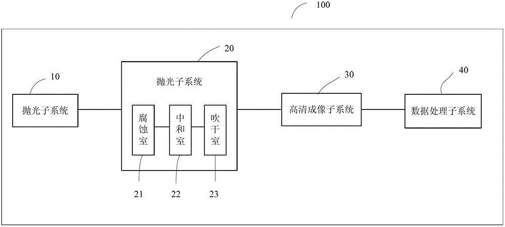
[0046] (1) Take a 156mm×156mm×230mm polysilicon block, polish it to a surface roughness value of Ra=0.2, etch the surface of the polished polysilicon block with an etching solution for 5 minutes to show the dislocation or defect of the silicon block, After the corrosion time is up, stop the corrosion with 1% NaOH solution, wash the polysilicon block with water and spray it to dry;

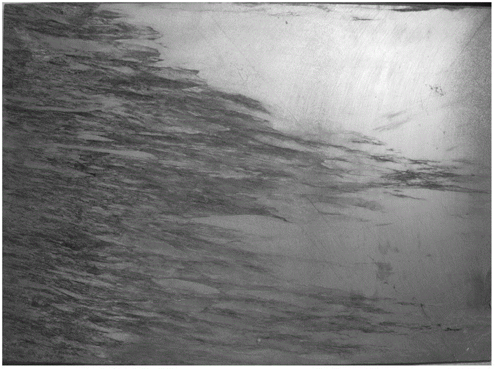
[0047] (2) Using a high-definition imaging system to image the surface dislocation of the obtained silicon block to obtain a corrosion image of the silicon block, so as to obtain the gray pixel ratio of the corrosion pit of the corrosion image according to the X, Y coordinates in the corrosion image and the corresponding pixel information;

[0048] (3) Measure the standard sample and establish the relational formula: take another 156mm×156mm×230mm polysilicon block, polish it to the surface roughnes...

Embodiment 2

[0058] A method for detecting dislocations in crystalline silicon, comprising the following steps:

[0059] (1) Take a 125×125×280mm polysilicon block, polish it to a surface roughness value of Ra=0.2, etch the surface of the polished polysilicon block with an etching solution for 10 minutes to show dislocations or defects of the silicon block, After the corrosion time is up, stop the corrosion with 1% NaOH solution, wash the polysilicon block with water and spray it to dry;

[0060] (2) Using a high-definition imaging system to image the surface dislocation of the obtained silicon block to obtain a corrosion image of the silicon block, so as to obtain the gray pixel ratio of the corrosion pit of the corrosion image according to the X, Y coordinates in the corrosion image and the corresponding pixel information;

[0061] (3) According to the relationship between the gray scale pixel ratio of corrosion pits obtained in Example 1 and the dislocation density value: dislocation de...

Embodiment 3

[0067] A method for detecting dislocations in crystalline silicon, comprising the following steps:

[0068] (1) Take a 125×125×280mm polysilicon block, polish it to a surface roughness of Ra=0.1, etch the surface of the polished polysilicon block with an etching solution for 20 minutes, to show dislocations or defects of the silicon block, After the corrosion time is up, stop the corrosion with 1% NaOH solution, wash the polysilicon block with water and spray it to dry;

[0069] (2) Using a high-definition imaging system to image the surface dislocation of the obtained silicon block to obtain a corrosion image of the silicon block, so as to obtain the gray pixel ratio of the corrosion pit of the corrosion image according to the X, Y coordinates in the corrosion image and the corresponding pixel information;

[0070] (3) According to the relationship between the gray scale pixel ratio of corrosion pits obtained in Example 1 and the dislocation density value: dislocation density...


PUM


Abstract

The embodiment of the invention discloses a crystal silicon dislocation detection method, which comprises the following steps of: (1) polishing a crystal silicon sample to be detected, corroding the crystal silicon sample by using corrosive liquid, and finishing the corrosion; (2) imaging the crystal silicon to be detected by employing a high-definition imaging system to obtain a crystal silicon corrosion image, and thus obtaining a corrosion pit gray-scale pixel rate of the crystal silicon corrosion image; and (3) obtaining the dislocation density of the crystal silicon sample to be detected according to a relationship between the corrosion pit gray-scale pixel rate and a dislocation density value. In addition, the invention also discloses a crystal silicon dislocation detection system. By the crystal silicon dislocation detection method and the crystal silicon dislocation detection system, the large-dimension crystal silicon can be directly detected, an intuitive dislocation result can be obtained, the detection method is simple and reliable, and a novel method is provided for observing dislocation of the crystal silicon.

Description

technical field [0001] The invention relates to the field of semiconductor manufacturing, in particular to a detection method and detection system for crystalline silicon dislocations. Background technique [0002] With the vigorous development of the solar photovoltaic industry, polycrystalline silicon solar cells have gradually become the mainstream of the market. More than 50% of polysilicon solar cells currently on the market are made of cast polysilicon. However, crystal defects in cast polysilicon, such as dislocations, grain boundaries, and micro-defects, are important factors that affect the conversion efficiency of solar cells. [0003] At present, the detection methods for the internal defects of semiconductors such as polycrystalline silicon block mainly include light irradiation detection method, infrared detection method, ultrasonic detection method, corrosion method and so on. However, the operation of these detection methods is not convenient enough, the equ...

Claims


Application Information

Patent Timeline
Patent Type & Authority Applications(China)
IPC IPC(8): G01N21/88G01N1/32
Inventor 何亮张涛胡动力雷琦黄雪雯
Owner JIANGXI SAI WEI LDK SOLAR HI TECH CO LTD
Why Eureka
Try Eureka