

Thin-film transistor, manufacture method of thin-film transistor, array substrate and display device
A technology for thin film transistors and array substrates, which is applied in the manufacture of transistors, semiconductor/solid-state devices, semiconductor devices, etc., can solve the problem of not effectively blocking hydrogen and water vapor from diffusing into the active layer, destroying the electrical properties of oxide transistors, and oxides Transistor threshold voltage drift and other issues, to achieve the effect of good compactness, good adjustment, and stable electrical performance
- Summary
- Abstract
- Description
- Claims
- Application Information
AI Technical Summary
Problems solved by technology
Method used
Image

Examples
Embodiment 1
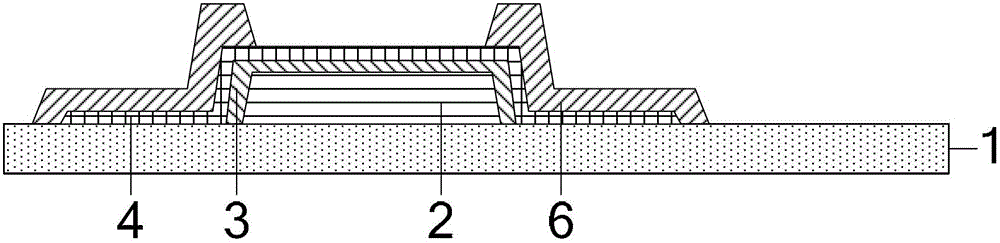
[0042] Corresponding to the above TFT, the present invention also provides an array substrate, such as Figure 4 As shown, at least one TFT is included; the TFT includes: a substrate 1 and a gate 2 sequentially arranged on the substrate 1, a first gate insulating layer 3, an active layer 4, an etching stopper layer 5, and source and drain electrodes layer 6, passivation layer 7 and pixel electrode 8; the first gate insulating layer 3 wraps the gate 2, the active layer 4 wraps the first gate insulating layer 3, and the first The material of the gate insulating layer 3 includes aluminum oxide.
[0043] A gate 2 comprising aluminum is disposed above the substrate 1; a first gate insulating layer 3 comprising aluminum oxide, an active layer 4 and an etching stopper layer 5 are disposed sequentially on the gate 2 from bottom to top;
[0044] The first gate insulating layer 3 containing aluminum oxide wraps the gate 2 and is formed by performing an in-situ reaction on the gate 2 co...
Embodiment 2
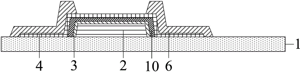
[0059] According to the array substrate described in Embodiment 1, when the first gate insulating layer 3 made of aluminum oxide is charged, more interface charges tend to appear on the first gate insulating layer 3, which easily causes the first The breakdown of the gate insulating layer 3 makes the gate 2 on both sides and the active layer 4 conduct, and damages the array substrate of the TFT.
[0060] In order to solve the above problems, preferably, such as Image 6 As shown, a second gate insulating layer 10 is also provided between the first gate insulating layer 3 and the active layer 4; the second gate insulating layer 10 wraps the first gate insulating layer Layer 3, the material of the second gate insulating layer 10 includes aluminum oxynitride.
[0061] In the preparation process of the array substrate, after the first gate insulating layer 3 made of aluminum oxide is formed on the surface of the gate 2 containing aluminum, the first gate insulating layer is forme...
Embodiment 3
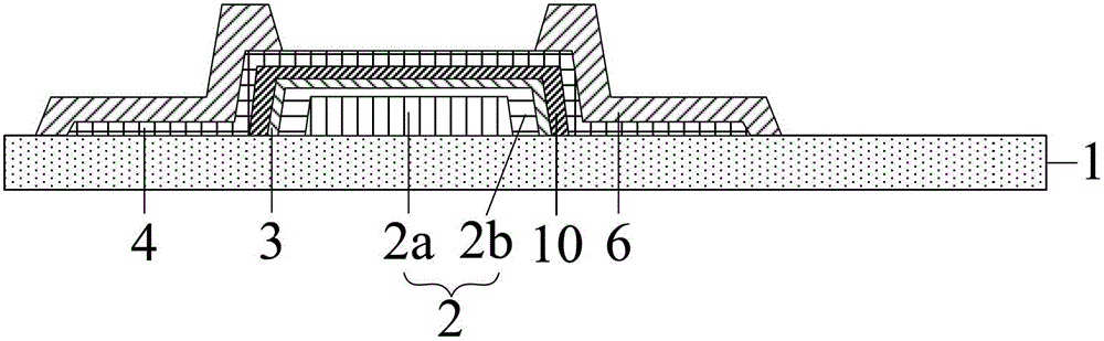
[0066] According to the array substrate described in Embodiment 1 or Embodiment 2, in order to further improve the conductivity of the gate 2, preferably, as Figure 7 As shown, the gate 2 is layered with an inner gate layer 2a and an outer gate layer 2b; the material of the inner gate layer 2a includes copper, and the material of the outer gate layer 2b includes aluminum.
[0067] In the manufacturing process, the inner gate layer 2a made of copper is firstly formed on the substrate 1 by deposition and etching; the outer gate layer 2b made of aluminum is formed by deposition and etching, wherein the outer gate layer 2b wraps Inner gate layer 2a.
[0068] After the gate 2 composed of the inner gate layer 2a and the outer gate layer 2b is formed, the outer gate layer 2a is directly subjected to an in-situ reaction to form the first gate insulating layer 3 made of aluminum oxide.
[0069] Because the conductivity of copper is better than that of aluminum, the conductivity of th...
PUM
| Property | Measurement | Unit |
|---|---|---|
| thickness | aaaaa | aaaaa |
| thickness | aaaaa | aaaaa |
| thickness | aaaaa | aaaaa |
Abstract
Description
Claims
Application Information