Flip chip packaging method
A technology of flip-chip packaging and chips, which is applied in the direction of electrical components, semiconductor/solid-state device manufacturing, circuits, etc., can solve problems such as insufficient peel strength and poor coating, so as to avoid insufficient peel strength, shorten sealing time, and improve sealing performance. The effect of glue efficiency
- Summary
- Abstract
- Description
- Claims
- Application Information
AI Technical Summary
Problems solved by technology
Method used
Image

Examples
Embodiment 1
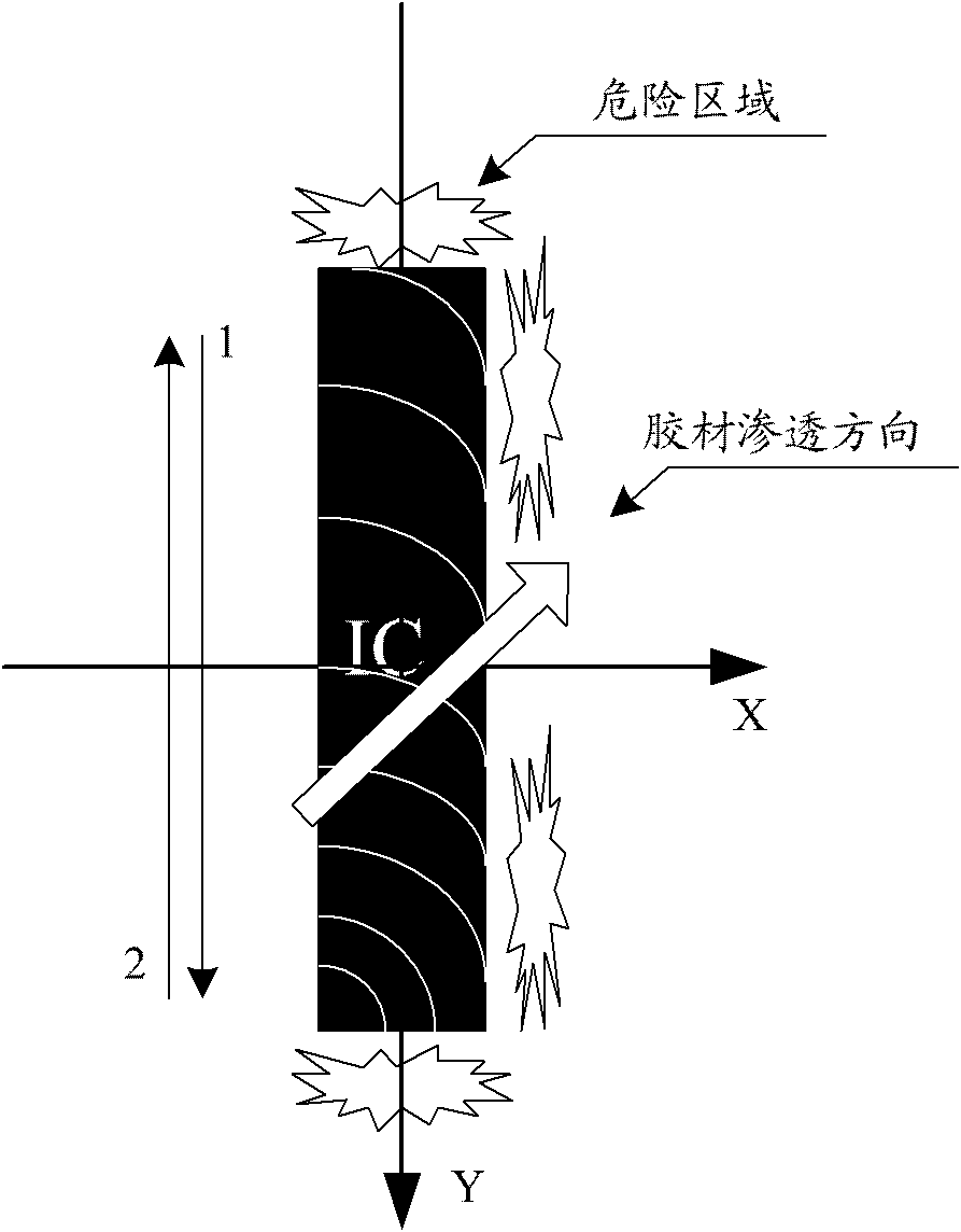
[0056] The specific process of the flip-chip packaging method disclosed in the embodiment of the present invention is as follows: figure 2 As shown, specifically, after the bumps of the chip IC are bonded to the pins of the circuit substrate, glue is applied around the chip, wherein the sequence of glue application is clockwise or counterclockwise along the circumference of the chip, and At least one side of the first long side of the chip is first coated with an adhesive material, and after the adhesive material seeps out from the bottom of the chip, the adhesive material is coated on the side of the second long side of the chip.
[0057] It should be noted that in this embodiment, as long as glue is applied around the chip in a clockwise or counterclockwise direction, the specific sequence of glue application is not limited, and glue can be applied from any position on the circumference of the chip, such as Glue can be applied from the short side of the chip, or from the lo...
Embodiment 2
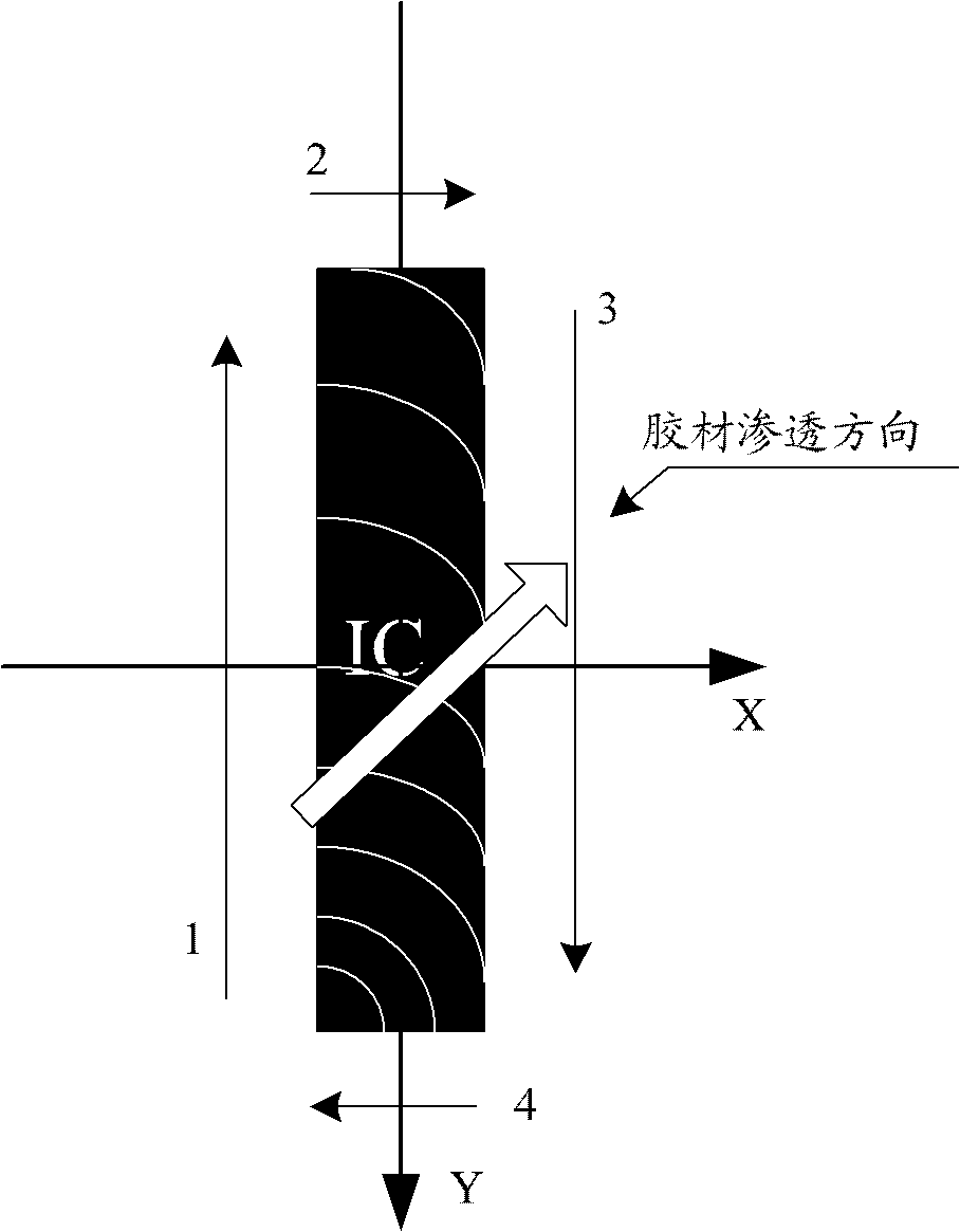
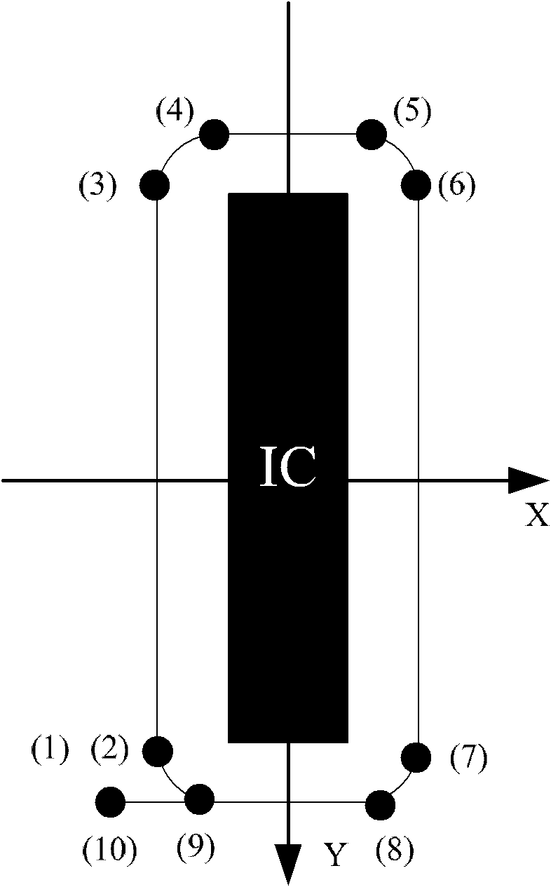
[0067] The specific process of the flip-chip packaging method disclosed in this embodiment is as follows: Figure 4 and Figure 5 as shown, Figure 4 Schematic diagram of the gluing path for the method, Figure 4 Each label in indicates the glue application direction and path, Figure 5 It is a schematic diagram of each coordinate point for determining the moving direction of the dispensing needle during the glue application process, Figure 5 The marks (1)-(10) in the figure represent each coordinate point, and the position of each coordinate point determines the moving direction of the dispensing needle.
[0068] It should be noted that, in general, the first long side coated in the glue coating process is the output terminal output of the chip, and the second long side is the input terminal input terminal of the chip, because there are often more pins at the output terminal of the chip. There are fewer pins at the input end, and the glue is applied from the output end w...
Embodiment 3
[0085] The specific process of the flip-chip packaging method disclosed in this embodiment is as follows: Figure 7 and Figure 8 As shown, similar to the previous embodiment, Figure 7 Schematic diagram of the gluing path for the method, Figure 7 Each label in indicates the glue application direction and path, Figure 8 It is a schematic diagram of each coordinate point for determining the moving direction of the dispensing needle during the glue application process, Figure 8 The reference numerals (1)-(11) in represent respective coordinate points.
[0086] In this embodiment, glue application from the output end of the chip is still taken as an example, that is, the long side on the left side of the chip in the figure is the output end of the chip, and the long side on the right side is the input end of the chip, and the points used in this embodiment The distance between the glue needle and the glue application path and the four sides of the chip is also similar to t...
PUM
| Property | Measurement | Unit |
|---|---|---|
| The inside diameter of | aaaaa | aaaaa |
| The inside diameter of | aaaaa | aaaaa |
Abstract
Description
Claims
Application Information
 - R&D Engineer
- R&D Manager
- IP Professional
- Industry Leading Data Capabilities
- Powerful AI technology
- Patent DNA Extraction
Browse by: Latest US Patents, China's latest patents, Technical Efficacy Thesaurus, Application Domain, Technology Topic.
© 2024 PatSnap. All rights reserved.Legal|Privacy policy|Modern Slavery Act Transparency Statement|Sitemap