
Novel fractal pattern grounding shield structure

A pattern ground shielding and shielding structure technology, applied in the direction of electrical components, electric solid devices, circuits, etc., can solve the problems of reducing the Q value of the inductor/transformer, reducing the L value of the inductor coil, and the energy loss of the substrate, so as to reduce the area, Increased working frequency, easy to achieve effect

Active Publication Date: 2012-10-17
HANGZHOU DIANZI UNIV
View PDF5 Cites 8 Cited by
  • Summary
  • Abstract
  • Description
  • Claims
  • Application Information

AI Technical Summary

Problems solved by technology

[0004] On-chip inductors / transformers are generally wound on a silicon substrate through a metal film, so they are a relatively open structure, and the electric and magnetic fields will permeate into the entire substrate during operation, so that in the substrate And the area on the surface of the substrate generates an induced current in the opposite direction, which will react on the metal coil, which will relatively reduce the L value of the inductor coil, and will also cause additional substrate energy loss, reducing the inductor / transformer Q value
If the electromagnetic field penetrating into the substrate can be effectively reduced, it will have a great impact on reducing loss, increasing the L value and Q value of the inductor / transformer coil and reducing the insertion loss IL of the transformer.

Method used


Image

  • Novel fractal pattern grounding shield structure
  • Novel fractal pattern grounding shield structure
  • Novel fractal pattern grounding shield structure

Examples


Embodiment Construction

[0025] The present invention will be further described below in conjunction with accompanying drawing.

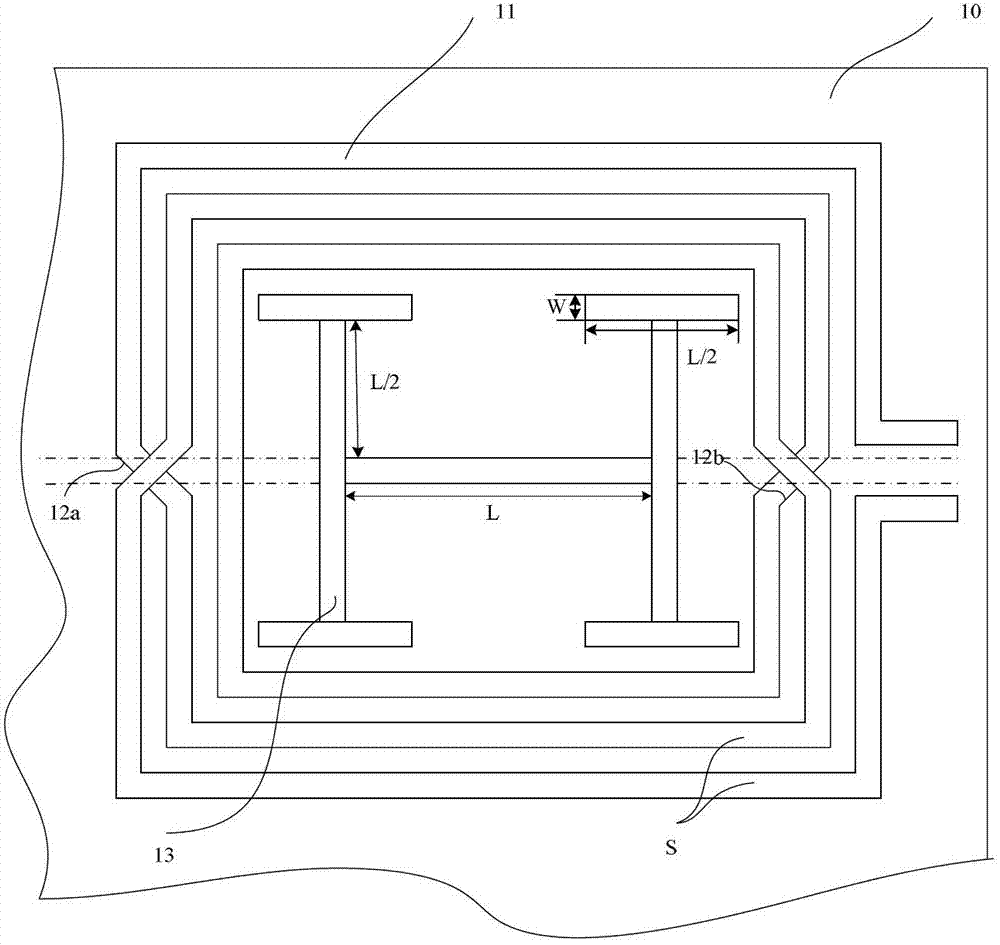
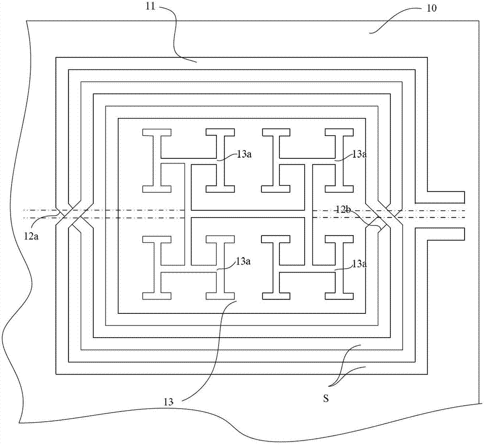
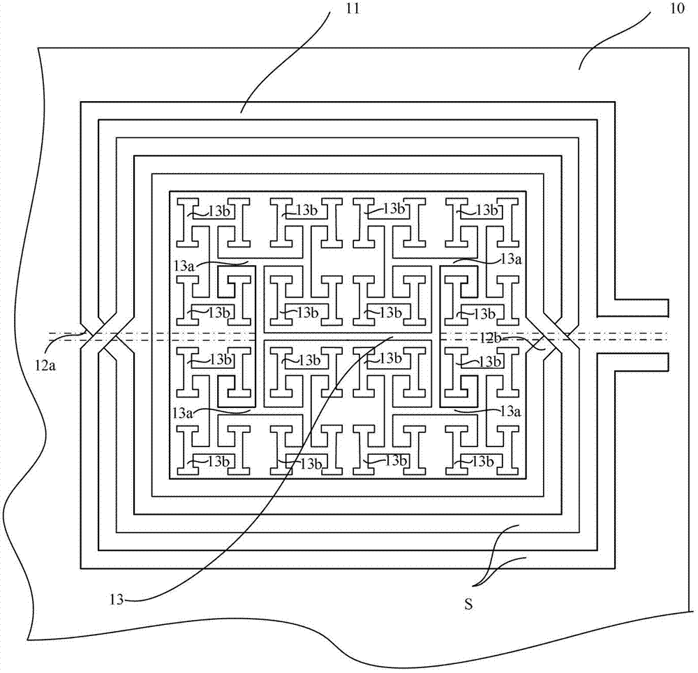
[0026] figure 1 It is a schematic plan view of an embodiment in which the first-order H-shaped fractal ground shielding structure of the present invention is applied to an inductor, such as figure 1 As shown, the inductance line 11 is wound from the top metal of the semiconductor substrate 10 (such as a silicon substrate), the inductance lines 12a and 12b are wound from the next top metal of the semiconductor substrate 10, and the inductance lines 11 and 12 are separated by air, and S is the distance between metal coils. In the central part of the inductor is an H-shaped first-order ground shielding basic unit 13 made of the underlying metal layer M1. The construction details of the basic unit 13: first select a center point, construct the horizontal metal strip with the length L and the width W in the middle of the H figure, the starting point is -L / 2, -W / 2, and the end ...


PUM


Abstract

The invention relates to a grounding shield structure which applies a fractal theory. In existing on-chip spiral inductors and transformers, because an alternating electromagnetic field is produced, induction current is produced on a substrate, energy loss is produced, and an induction value and a Q value are reduced. The shield structure is arranged in the center of an inductor / transformer which is wound from a coil, and a pattern grounding shield layer of a first order, a second order, a third order and even a higher order is constructed with metal layers M1 and M2 with thin bottom layers based on H-shaped and crisscross basic units through the self similarity and iterative principle of the fractal theory. According to the novel fractal pattern grounding shield structure, the electromagnetic field which penetrates to the substrate is effectively shielded, so that the induction current which can be produced on the substrate and on the surface area of the substrate is reduced, and the effects of reducing the energy loss of the substrate and improving the induction value and a quality factor are achieved.

Description

technical field [0001] The invention belongs to the technical field of integrated circuits, and in particular relates to a novel grounding shielding structure applying fractal theory, and the fractal shielding grounding structure is mainly used in unit circuits of radio frequency integrated circuits. Background technique [0002] With the rapid development of CMOS radio frequency integrated circuits, the requirements for high performance / low power consumption / integration are getting higher and higher. Unit circuits such as low noise amplifiers, voltage controlled oscillators, mixers, intermediate frequency filters, power amplifiers, etc. are the basis for the success of the entire circuit, and the on-chip inductor / transformer is an essential component. Therefore, its design And optimization has become one of the keys to the successful design of the whole circuit. [0003] An important index to evaluate the performance of inductors / transformers is the quality factor Q, which...

Claims


Application Information

Patent Timeline
Patent Type & Authority Applications(China)
IPC IPC(8): H01L23/552
Inventor 孙玲玲刘军赵倩
Owner HANGZHOU DIANZI UNIV
Learn More