Detector pixel signal readout circuit and imaging method thereof

A technology for reading out circuits and image signals, which can be used in image communication, television, electrical components, etc., and can solve problems such as limited applications, expensive systems, and complexity

Active Publication Date: 2018-02-16
半导体器件有限公司
View PDF4 Cites 0 Cited by
  • Summary
  • Abstract
  • Description
  • Claims
  • Application Information

AI Technical Summary

Problems solved by technology

This makes such systems generally more expensive and complex, limiting their application in the field

Method used


Image

  • Detector pixel signal readout circuit and imaging method thereof
  • Detector pixel signal readout circuit and imaging method thereof
  • Detector pixel signal readout circuit and imaging method thereof

Examples


Embodiment Construction

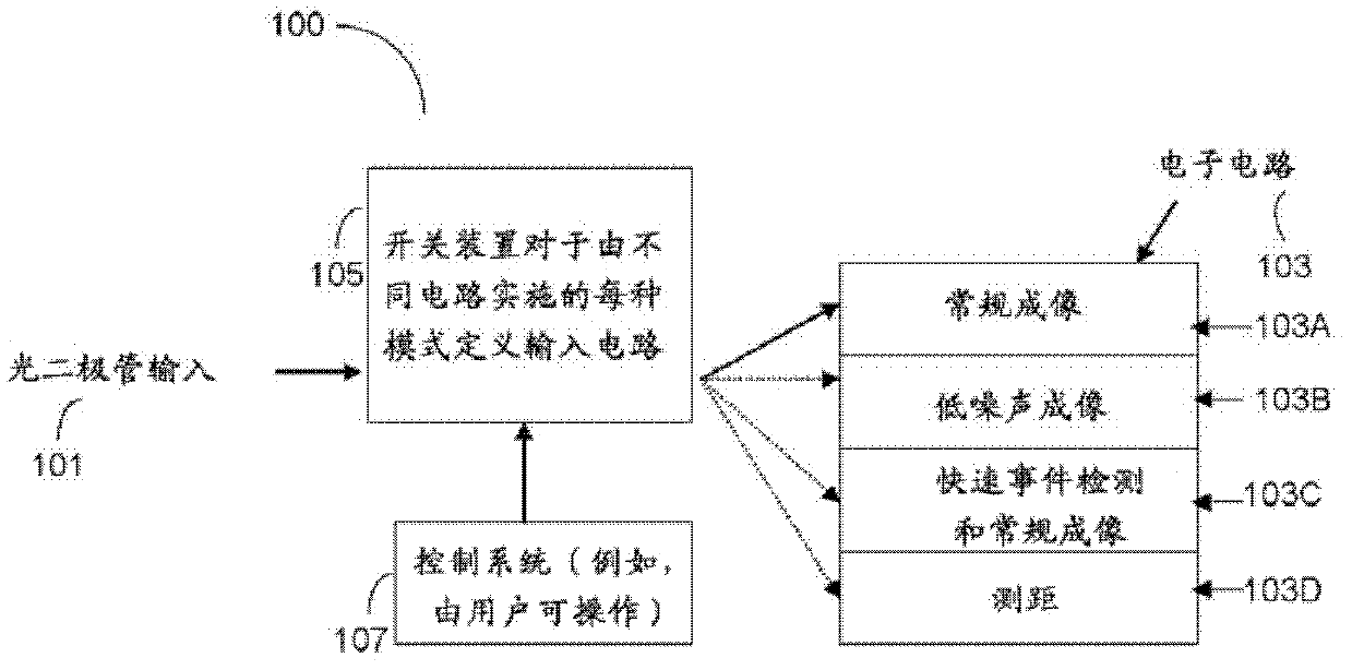
[0058] The present invention provides pixel readout circuitry integrated in an imaging pixel array, where the readout circuitry can implement (i.e., by processing the same frame of data) specific modes simultaneously or nearly The characteristics of the input signal to the readout circuit, or may depend on the characteristics of the output signal desired by the readout circuit.

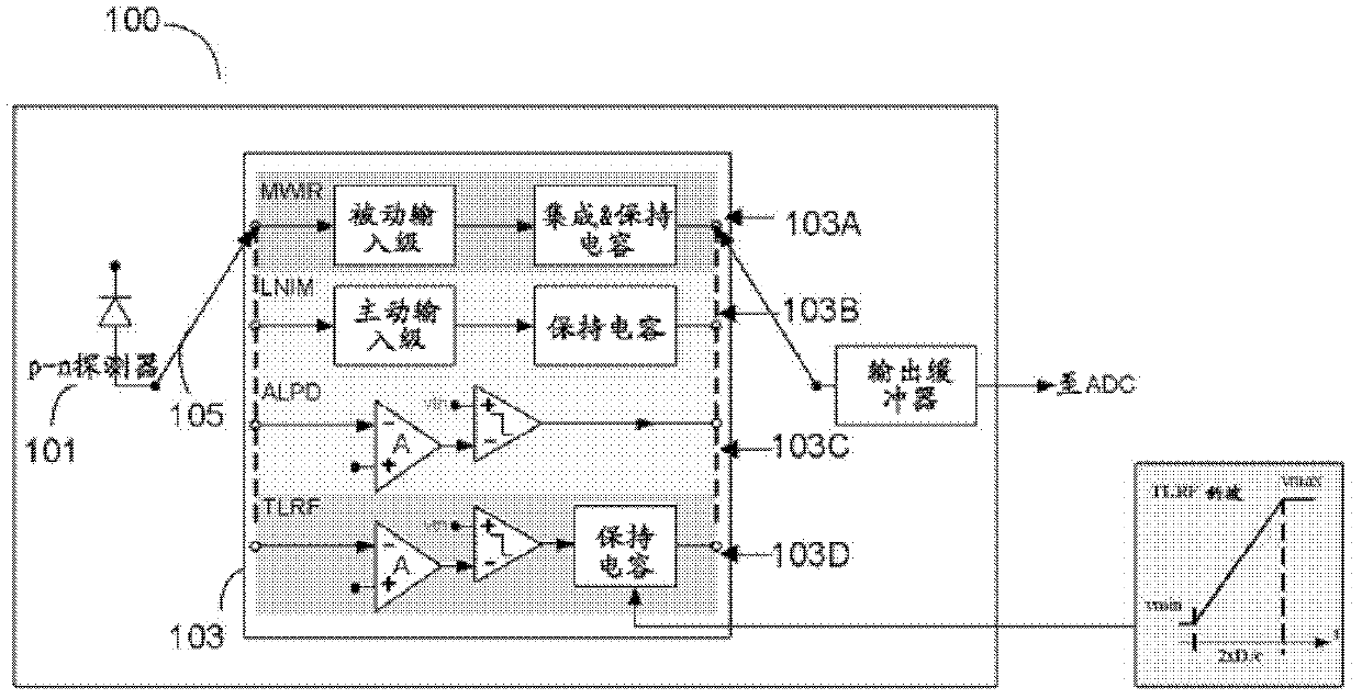
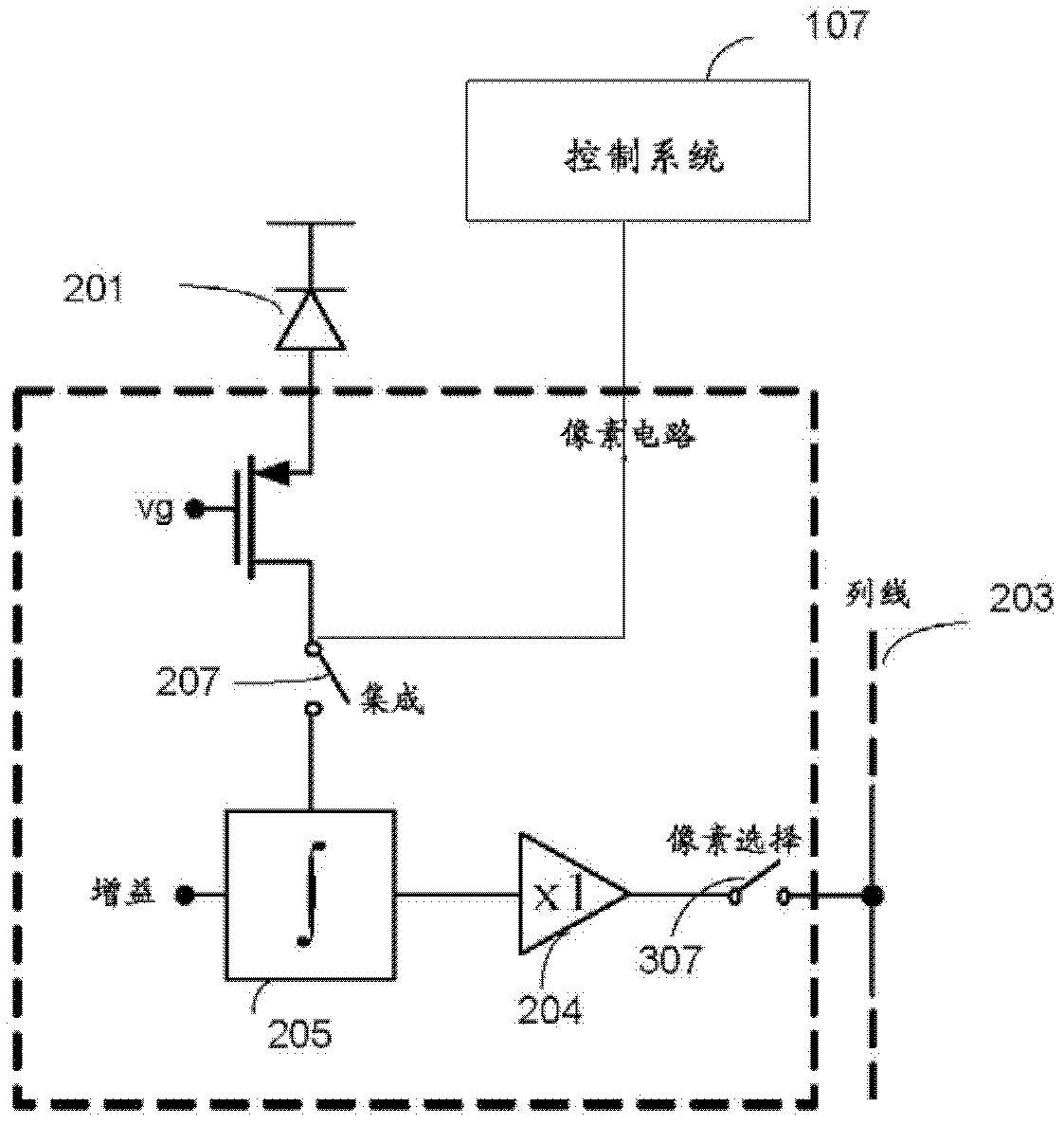
[0059] see Figure 1A , illustrating the integration of the pixel readout circuit 100 in any type of active matrix photodetector (diode array). For example, active matrix photodetectors are available in different types of InSb FPAs in 320x256, 480x384 and 640x512 element formats with pitches ranging from 15-30µm. The diode array may be InSb diodes produced in the process described in [1] (planar technology). To enable various functions of the ROIC, the pixel circuit of the present invention includes a set of switches, capacitors, amplifiers and memories. By controlling the switches and the bias lev...


PUM


Abstract

A pixel readout circuit for an imaging pixel array, the pixel readout circuit comprising: an input channel for receiving an image signal corresponding to an electrical output of a photosensitive element of a pixel; and an interconnection between the input channel and an output readout facility A circuit comprising a capacitor unit and a signal analyzer. Said capacitive units are controllably linked to input channels for accumulating charges corresponding to received intensities produced by the pixels during a single frame, and to output readout facilities for transferring image data thereto. said signal analysis unit is controllably linked to said input channel for receiving and analyzing at least part of said image signal produced by said pixels during a single frame period, and is connected to said output readout facility, said The signal analysis unit is configured and operable to analyze at least a portion of the image signal by determining an amount of accumulated charge corresponding to the received intensity, and upon detecting that the amount of accumulated charge satisfies a predetermined condition, generating an indication of the Data for an event is generated and the data is sent to the output reading facility.

Description

technical field [0001] The invention relates to the field of detector pixel signal readout and processing. [0002] quote [0003] The following references are considered relevant for understanding the background of the invention: [0004] 1: I.O.Nesher and P.Klipstein, "High performance IR detectors at SCDpresent and future", SPIE Annual Report, Volume 5957, Infrared Optoelectronics, August 2005, pages 0S1-OS12 Background technique [0005] The photodetector device responds to received photons by creating an electrical effect that can be quantified and thus provide information about the flux of the received photons. A focal plane array (FPA) of detectors is used to obtain an image of the object, so each detector provides a pixel in the image array. In this image, each pixel is provided with a unique address and value, which can be further used to process the image to extract information from the image. [0006] The coordination between imaging parameters is a trade-off ...

Claims


Application Information

Patent Timeline
Patent Type & Authority Patents(China)
IPC IPC(8): H04N5/343H04N5/335H04N5/3745
CPCH04N25/42H04N25/00H04N25/77H04N5/33
Inventor S·埃尔坎E·伊兰R·多布鲁密斯林
Owner 半导体器件有限公司
Why Eureka
Try Eureka