Supercharge Your Innovation With Domain-Expert AI Agents!

PCB (Printed Circuit Board) microstrip printed inductor

A printed circuit board and inductance technology, applied in the field of inductance, can solve the problem of difficult to find inductive components, and achieve the effect of ensuring stable transmission, improving product production efficiency, and reducing material costs and labor costs

Inactive Publication Date: 2012-10-17
SHENZHEN GONGJIN ELECTRONICS CO LTD
View PDF2 Cites 3 Cited by
  • Summary
  • Abstract
  • Description
  • Claims
  • Application Information

AI Technical Summary

Problems solved by technology

However, inductors are non-standard components, and it is difficult to find device manuals for inductor components

Method used


Image

  • PCB (Printed Circuit Board) microstrip printed inductor
  • PCB (Printed Circuit Board) microstrip printed inductor

Examples


Embodiment Construction

[0009] The present invention is described in further detail below in conjunction with accompanying drawing:

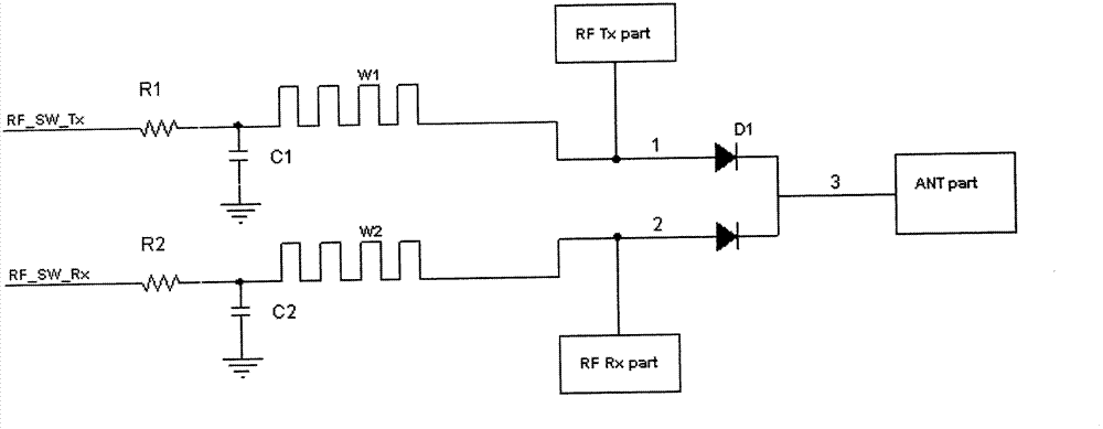
[0010] Such as figure 1 As shown, the PCB printed microstrip inductor of the present invention is a section of copper-clad microstrip line printed on a PCB printed circuit board. The microstrip line is a serpentine microstrip line, which can also be called a rectangular wave microstrip line.

[0011] Such as figure 2 As shown, there are two microstrip lines, one end is connected to the radio frequency circuit Tx switch control signal --- RF_SW_Tx, and the other end is connected to the radio frequency transmission circuit --- RF Tx part or connected to the antenna through the duplex tube D1 --- ANT, the other end is connected to the RF circuit Rx switch control signal --- RF_SW_Rx and the other end is connected to the RF receiving circuit --- RF Rx par or connected to the antenna through the duplex tube D1 --- ANT.

[0012] The present invention simulates through sim...


PUM


Abstract

The invention discloses a PCB (Printed Circuit Board) microstrip printed inductor. The PCB microstrip printed inductor comprises a section of a copper-clad microstrip line printed on a PCB, wherein the copper-clad microstrip line is a serpentine microstrip line. By replacing an inductive component with the microstrip line formed through wiring the PCB, the PCB microstrip printed inductor has the advantages that the effect of filtering radio-frequency (RF) switching signals is exerted so as to ensure the stability of RF switching control signals; compared with RF Tx and RF Rx signals, the printed inductor is of a high-impedance state and can effectively isolate RF signals, so that the RF signals of transmission attenuation are avoided, and the stability in transmission of the RF signals is ensured; the microstrip printed inductor can be formed through together simulation, can be set to have any inductance value theoretically, and can then avoid the limitation of the inductance value when the inductive component is selected; and the materiel cost and the labor cost can be effectively reduced, and the production efficiency of products is increased.

Description

technical field [0001] The invention relates to an inductor, in particular to a PCB printed microstrip inductor. Background technique [0002] In radio frequency circuits with frequencies below 2 GHz, the distribution parameter size is often too large, which is inconvenient to use in many occasions. The small size of integrated components allows them to be used in a wide range of active and passive circuits. However, inductors are non-standard components, and it is difficult to find device manuals for inductor components. How to make high-quality inductive components is an important issue in radio frequency circuits. It is particularly important to select the inductance in the RF switch circuit. The selected inductance must be able to filter the RF switch control signal and have no effect on the RF signal (receiving and transmitting signals) of the RF circuit. Contents of the invention [0003] The technical problem to be solved by the present invention is to provide a ...

Claims


Application Information

Patent Timeline
Patent Type & Authority Applications(China)
IPC IPC(8): H05K1/16
Inventor 刘克文王金桂
Owner SHENZHEN GONGJIN ELECTRONICS CO LTD
Features
  • R&D
  • Intellectual Property
  • Life Sciences
  • Materials
  • Tech Scout
  • Unparalleled Data Quality
  • Higher Quality Content
  • 60% Fewer Hallucinations
Learn More