Bonding device for polymer microfluidic chip

A microfluidic chip and bonding device technology, applied in the controllable bonding equipment and precision fields, can solve the problems of poor mask versatility, high cost, complex manufacturing process, etc., and achieve precise positioning, high-precision temperature monitoring and Control and realize the effect of automatic self-locking and clamping

Inactive Publication Date: 2012-10-31
SUZHOU UNIV
View PDF3 Cites 5 Cited by
  • Summary
  • Abstract
  • Description
  • Claims
  • Application Information

AI Technical Summary

Problems solved by technology

However, with the gradual reduction of the manufacturing cost of polymer micro-devices, the proportion of packaging costs continues to rise. According to a number of foreign statistics, the cost of polymer micro-device packaging accounts for 50% to 90% of its products, and product problems About 80% is due to encapsulation
[0007] Applying the laser mask welding method to the bonding of PMMA microfluidic chips with a thickness of 0.1-2.5 mm, a non-leakage microchip with a weld width of 175 μm can be obtained, indicating that laser transmission welding is bonded to polymer microfluidic chips. However, the masks have poor versatility, complex manufacturing process and high cost. Microfluidic chips with different structures must be equipped with different masks to adapt to the changes in the microchannels in the microchip.
[0008] Due to the limitations of the current bonding methods for various polymer microfluidic chips, how to obtain a weld with a narrower width, smaller heat-affected zone, and higher strength than laser mask bonding is an important task in this field. Technical issues resolved

Method used


Image

  • Bonding device for polymer microfluidic chip
  • Bonding device for polymer microfluidic chip

Examples


Embodiment 1

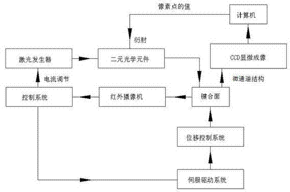
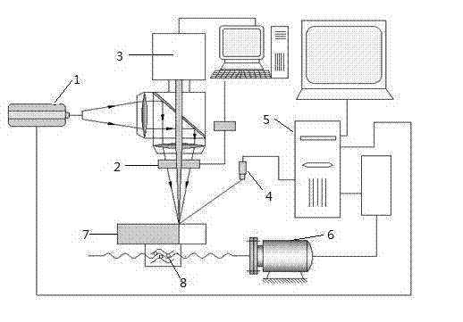
[0025] Embodiment 1: A polymer microfluidic chip bonding device, including a laser generator, a controllable optical system containing a liquid crystal mode micro-optical device, an image recognition and image processing system, an online real-time temperature monitoring and control system, and a precision displacement Control platform, servo drive system and control system.

[0026]

[0027] See attached figure 1 As shown, in the controllable optical system, there is a binary optical element 2 in liquid crystal mode, and the laser beam is diffracted by the binary optical element 2 at the chip to be bonded on the displacement control platform 7; the image recognition and processing The system includes a CCD3 and a computer, and the size and intensity of the light spot can be flexibly controlled by the computer processing the diffraction image collected by the CCD3.

[0028] The temperature online real-time monitoring and control system includes an infrared camera 4 with a wa...


PUM


Abstract

The invention discloses a bonding device for a polymer microfluidic chip, comprising a laser generator, a controllable optical system, an image identification and image processing system, a control system, and a displacement control platform. The bonding device is characterized in that a binary optical element is arranged in the controllable optical system, a laser beam is diffracted at a to-be-bonded chip on the displacement control platform via the binary optical element, and the formed optical spots are controllable in size and intensity; and the image identification and image processing system is arranged, the image identification and image processing system comprises a CCD (charge coupled device) and a computer, and the sizes and intensities of the optical spots are controlled via the processing of the computer on the acquisition of the CCD for the diffracted images. According to the invention, a binary optical technology, a polymer laser transmission welding technology, and a real-time online temperature and image measurement technology are combined together; and welding seams which are narrower in bonding width, smaller in a heat affected zone, and higher in intensity compared with a laser mask can be obtained by virtue of the diffraction action of the binary optical element on laser.

Description

technical field [0001] The invention relates to a microfluidic chip bonding equipment, in particular to precise and controllable bonding equipment for a microfluidic chip. Background technique [0002] Microfluidic chip, also known as micro-total analysis system or lab-on-a-chip, is a process of sample preparation, biological and chemical reactions, separation and detection involved in the fields of chemistry and biology, which is miniaturized or basically miniaturized to a few On a chip of square centimeters, and the technology of detecting and analyzing the results. Compared with the traditional analysis technology, the microfluidic chip is a "micro" and "complete" analysis technology platform, and it is also the focus of the development of the current micro-complete analysis system. [0003] In recent years, with the wide application of polymer materials, some plastics with biochemical compatibility and easy mass production by means of precision injection molding and hot...

Claims


Application Information

Patent Timeline
Patent Type & Authority Applications(China)
IPC IPC(8): B29C65/16
Inventor 王传洋
Owner SUZHOU UNIV
Why Eureka
Try Eureka