System and method for actively correcting offset drift and wire bonder

A wire bonding machine and biasing technology, which is applied in the manufacture of electrical components, electrical solid devices, semiconductor/solid devices, etc., can solve the problems of low measurement accuracy and sensitivity, complex system structure, and difficult installation, and achieve simple structure, Ensure the effect of welding precision and low cost

Inactive Publication Date: 2014-07-16
CETC BEIJING ELECTRONICS EQUIP
View PDF3 Cites 0 Cited by
  • Summary
  • Abstract
  • Description
  • Claims
  • Application Information

AI Technical Summary

Problems solved by technology

[0007] However, the existing technical solutions for measuring and correcting the distance offset drift between the chopper and the imaging system 2 have low measurement accuracy and sensitivity in specific applications, and the system structure is complicated, difficult to install, and high in cost.

Method used


Image

  • System and method for actively correcting offset drift and wire bonder
  • System and method for actively correcting offset drift and wire bonder
  • System and method for actively correcting offset drift and wire bonder

Examples


Embodiment Construction

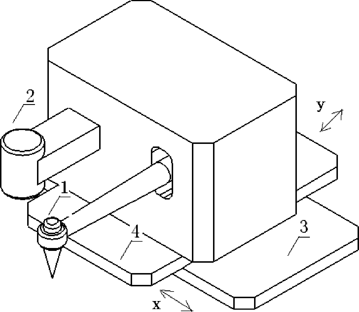
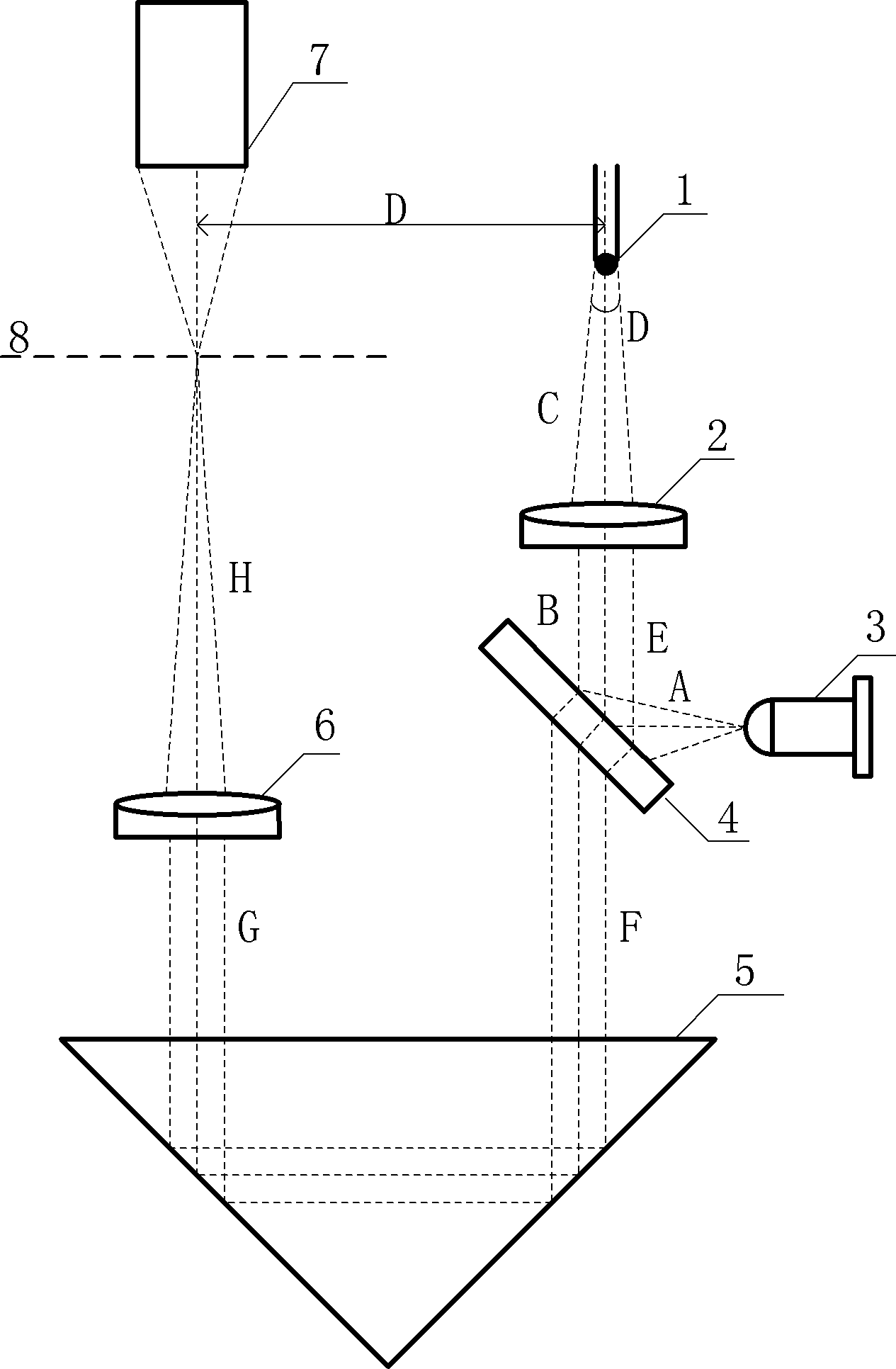
[0046] The embodiment of the present invention provides an active correction system for offset drift, which is installed on the semiconductor post-packaging equipment - wire bonder (Wire bonder), and is used to measure the temperature of the bonding head and other random errors of the system The distance between the capillary and the imaging system (that is, the optical system) in the wire bonding machine caused by the figure 2 D in ) indicates offset drift, and the distance parameter between the capillary and the imaging system is corrected, so that the wire bonding machine uses the current correct distance parameter between the capillary and the imaging system for welding.

[0047] The bias drift active correction system provided by the embodiments of the present invention can realize precise, high-speed, and stable chip bonding or real-time measurement of the bias drift of the imaging system and the chopper during bonding. The specific implementation of the system can be a...


PUM


Abstract

The invention provides a system and a method for actively correcting an offset drift and a wire bonder. Collimating mirrors, a spectroscope, a coaxial-light emitter and a back reflector are arranged reasonably; a difference value of different positions, on a target surface of an imaging system detector, of a metal ball formed by a capillary tip at different time points during work is determined as offset drift amount of the distance between the capillary and the imaging system; and a parameter about the distance between the capillary and the imaging system is corrected according to the offset drift amount. The offset drift amount of the distance between the capillary and the imaging system can be accurately measured and corrected in real time, so that welding accuracy of the wire bonder is guaranteed, and rate of finished chip is increased. Besides, the system for actively correcting the offset drift and the wire bonder are simple in structures, low in cost and convenient to modularize.

Description

technical field [0001] The invention relates to the technical field of semiconductor device production technology, in particular to an offset drift active correction system, method and wire bonding machine. Background technique [0002] The electrical performance of semiconductor devices, such as integrated circuit chips, is generally achieved by bonding the chip to the lead frame, and then through wire bonding or flip-chip welding (connecting the solder joints of the chip to the pins of the material frame). [0003] The process of wire bonding is to first place gold wires to the pads on the chip, and then connect the pads to the leads of the lead frame. When all the solder joints and pins are bonded together, they are packaged to form an integrated circuit chip. Usually the package is a ceramic package or a plastic package. Common chips generally have hundreds or even thousands of solder joints that need to be connected. [0004] There are many types of wire bonding equi...

Claims


Application Information

Patent Timeline
Patent Type & Authority Patents(China)
IPC IPC(8): H01L21/68H01L21/00H01L21/60H01L21/66
CPCH01L2224/78H01L24/78H01L2924/12041H01L2924/00014H01L2224/48H01L2924/00H01L2924/00012
Inventor 于丽娜王双全
Owner CETC BEIJING ELECTRONICS EQUIP
Why Eureka
Try Eureka