Integrally-packaged power semiconductor device

A technology of power semiconductors and devices, which is applied in the direction of semiconductor devices, semiconductor/solid-state device components, electric solid-state devices, etc., can solve the problems of difficult chip flipping and installation, and the inability to obtain exposed chip bases, etc., to achieve the effect of improving product performance

Active Publication Date: 2012-10-31
ALPHA & OMEGA SEMICON INT LP
View PDF3 Cites 23 Cited by
  • Summary
  • Abstract
  • Description
  • Claims
  • Application Information

AI Technical Summary

Problems solved by technology

Therefore, it is difficult to flip and install the chip in this package structure so that the source on the upper surface is connected to the chip base, and it is impossible to obtain the above-mentioned exposed chip base as the ground electrode and the effect of helping heat dissipation.

Method used


Image

  • Integrally-packaged power semiconductor device
  • Integrally-packaged power semiconductor device
  • Integrally-packaged power semiconductor device

Examples


Embodiment 1-1

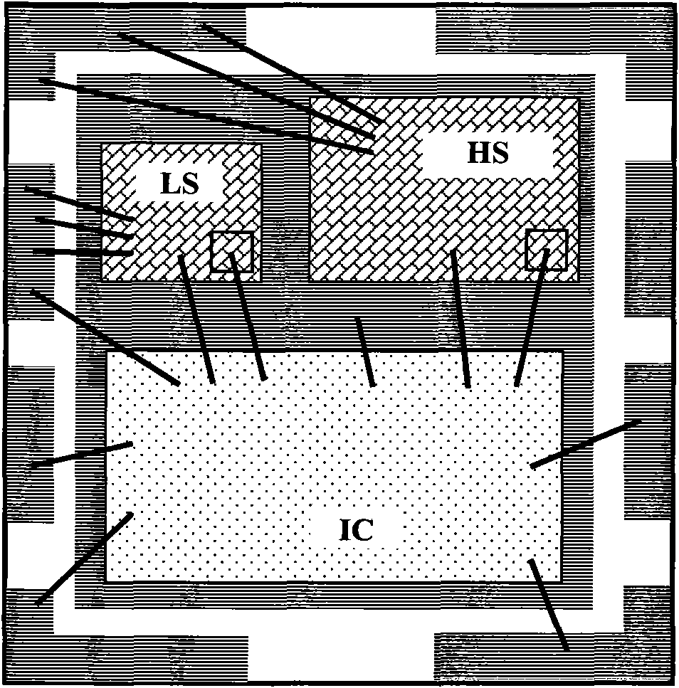
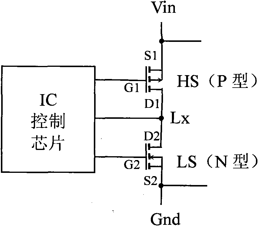
[0081] Please refer to figure 2 , Figure 4 , Figure 6 Shown is an implementation structure of the power semiconductor device of the present invention, wherein Figure 4 is a schematic diagram of the overall structure of the power semiconductor device, Figure 6 yes Figure 4 Sectional view of position A-A in the center. correspond figure 2 It can be seen from the schematic circuit diagram that the P-type high-end MOSFET chip 30 , the N-type low-end MOSFET chip 20 and the control chip 40 are jointly packaged in the power semiconductor device.

[0082] The power semiconductor device includes a lead frame, on which a chip base 100 is arranged, and several pins separated from the chip base 100 and not electrically connected.

[0083] The high-end and low-end MOSFET chips are respectively provided with a bottom drain, a top source, and a top gate; correspondingly, the plurality of pins include a high-end source pin 72, a low-end gate pin 71, a switch pin 74 and several c...

Embodiment 1-2

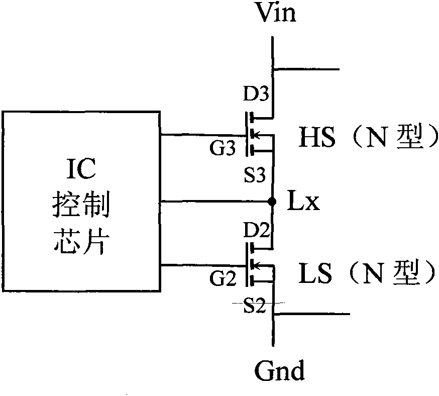
[0095] Please refer to image 3 , Figure 5 , Figure 6 , Figure 7 shown, where Figure 5 is a schematic diagram of the overall structure of the power semiconductor device, Figure 6 yes Figure 5 The cross-sectional view of the A-A position in the middle, Figure 7 yes Figure 5 Sectional view of position C-C in middle. correspond image 3 It can be seen from the schematic circuit diagram that the control chip 40 and N-type high-end and low-end MOSFET chips are jointly packaged in the power semiconductor device.

[0096] The chip base 100 described in this embodiment and the lead frame structure of several pins separated therefrom are the same as in the above-mentioned embodiment; The same applies to the examples. A brief description is as follows:

[0097] Cooperate see Figure 5 , Figure 6 and Figure 8 As shown, the low-side MOSFET chip 20 is turned over and bonded on the chip base 100, its top source 22 is electrically connected to the chip base 100, and i...

Embodiment 2-1

[0105] Please refer to figure 2 , Figure 9 , Figure 11 shown, where Figure 9 is a schematic diagram of the overall structure of the power semiconductor device, Figure 11 yes Figure 9 Sectional view of the B-B position in the middle. correspond figure 2 It can be seen from the schematic circuit diagram that the P-type high-end MOSFET chip 30 , the N-type low-end MOSFET chip 20 and the control chip 40 are jointly packaged in the power semiconductor device.

[0106] Similar to Embodiment 1-1, in this embodiment, a control chip 40 is provided at one end of the chip base 100 of the lead frame, and an inverted low-end MOSFET chip 20, a first metal connecting plate 51, The high-side MOSFET chip 30 and the second metal connecting plate 52 . Wherein, the first metal connecting plate 51 is electrically connected to the bottom drains 23 and 33 of the high-side and low-side MOSFET chips on its top surface and bottom surface, respectively, and is connected to the switch pin 7...


PUM


Abstract

The invention relates to an integrally-packaged power semiconductor device. A top source electrode of an inverted low-end MOSFET (Metal-Oxide-Semiconducotr Field Effect Transistor) chip is electrically connected to the top surface of a chip base; a bottom drain electrode of a high-end MOSFET chip or a top source electrode of the inverted high-end MOSFET is electrically connected with a bottom drain electrode of the low-end MOSFET chip through a first metal connecting plate; a second metal connecting plate is stacked on the high-end MOSFET chip; and the chip base is also provided with a control chip and is electrically connected with the electrodes of the high-end MOSFET chip and the low-end MOSFET chip. According to the invention, a plurality of chips are stereoscopically packaged so as to reduce the whole size of the semiconductor device; in addition, the product performance of the semiconductor device is improved by largening the size of each chip in a packaging body which has the same size as that of the chip; and because the top source electrode of the low-end MOSFET chip and the top surface of the chip base are connected, the bottom surface of the packaged and exposed chip base is connected with a ground electrode, and the shape of the exposed bottom surface is simplified, and the area of the exposed bottom surface is maximized so as to facilitate heat dissipation.

Description

technical field [0001] The invention relates to a power semiconductor device, in particular to a structure capable of jointly packaging multiple chips and other components in the same power semiconductor device. Background technique [0002] At present, in typical power semiconductor devices, MOSFET chips (metal oxide semiconductor field effect transistors) and control chips are usually packaged together in the same package to reduce the number of peripheral devices and improve the utilization efficiency of power supplies. [0003] For a DMOSFET (double-diffused metal oxide semiconductor tube) chip, if the source electrode on the upper surface of the chip can be connected to the chip base of the lead frame, the bottom surface of the chip base can be exposed as a ground electrode and For heat dissipation. [0004] The realization of the above packaging structure requires flipping the chip and installing it on the chip base, which will face the following problems: For example...

Claims


Application Information

Patent Timeline
Patent Type & Authority Applications(China)
IPC IPC(8): H01L23/538H01L23/495H01L23/36H01L25/04
CPCH01L2224/48091H01L2224/48137H01L2224/48247H01L2224/73221H01L2924/13091H01L2924/1306H01L2224/40095H01L2224/40245H01L24/40H01L2924/181H01L2224/371H01L2224/8385H01L2224/8485H01L2224/37H01L2224/40H01L2224/0603H01L2924/00014H01L2924/00H01L2924/00012
Inventor 何约瑟哈姆扎·依玛兹薛彦迅鲁军
Owner ALPHA & OMEGA SEMICON INT LP
Why Eureka
Try Eureka