Micro-nano processing method and device
A micro-nano processing and pre-processing technology, applied in the direction of electrolysis process, electrolysis components, etc.
- Summary
- Abstract
- Description
- Claims
- Application Information
AI Technical Summary
Problems solved by technology
Method used
Image

Examples
Embodiment 1
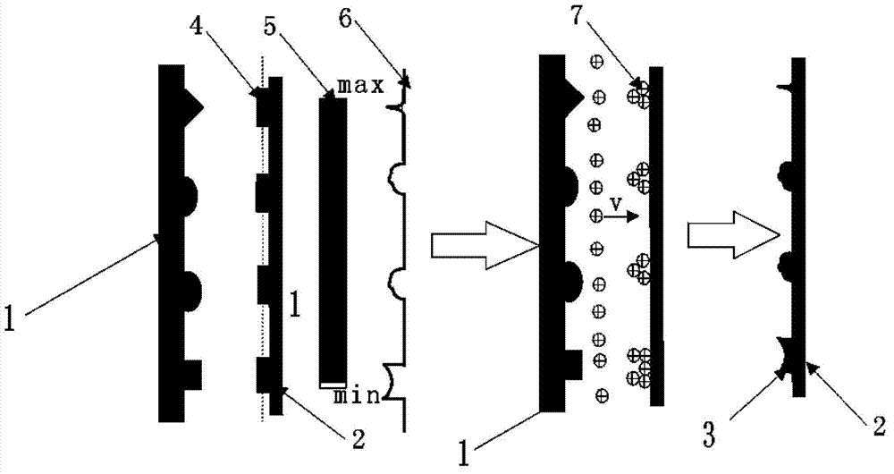
[0054] like figure 1 As shown, it is a schematic diagram of the principle of the electrochemical processing method of the micro-nano structure to control the distribution of the electrostatic field, where 1 is the electrode plate, 2 is the substrate to be processed, 3 is the micro-nano structure to be prepared, and 4 is the virtual electrostatic field on the substrate Nearby intensity distribution, 5 is the color scale of the electric field intensity, the darker the color, the stronger the field strength, 6 is the contour curve of the field intensity on a plane near the surface of the substrate to be processed (at the position of the dotted line), 7 is the electrochemical solution carriers in .
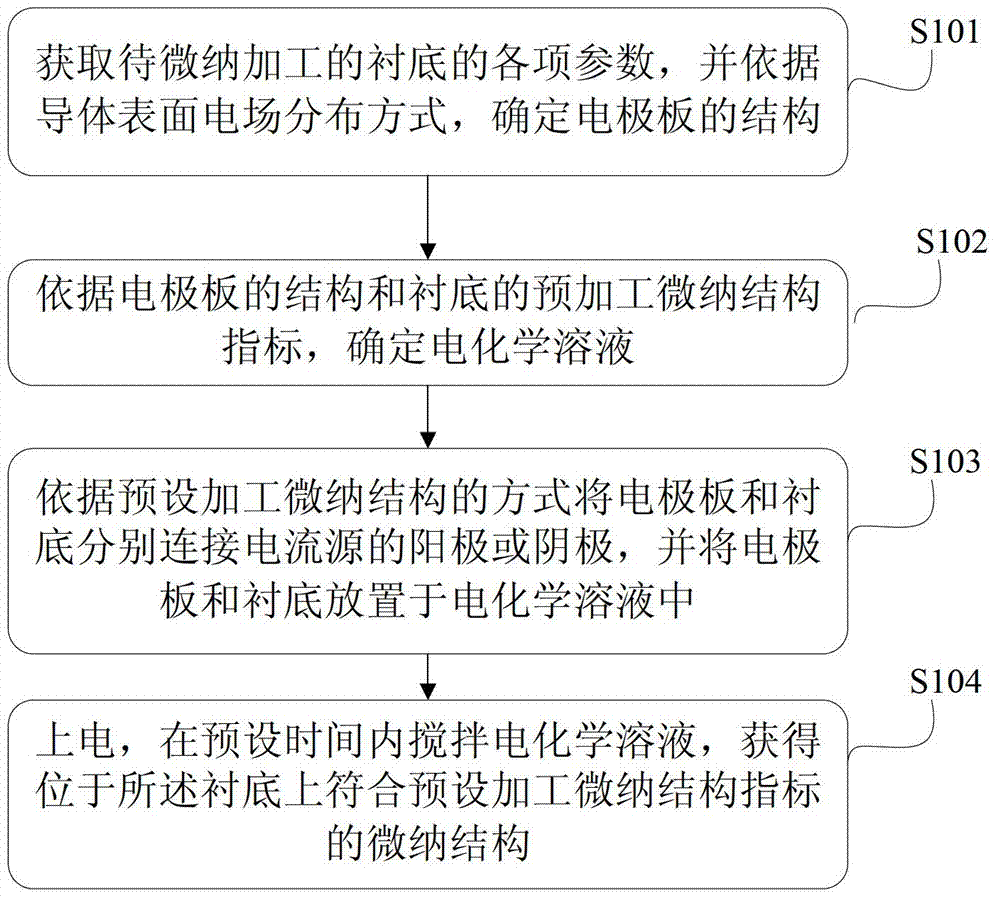
[0055] Based on the above structure, such as figure 2 As shown, it is a flowchart of a micro-nano processing method disclosed in the embodiment of the present invention, which mainly includes the following steps:
[0056] Step S101, obtaining various parameters of the substrate to ...
Embodiment 2
[0095] like Figure 5 As shown, it is a schematic structural diagram of a micro-nano processing device disclosed in this embodiment of the present invention, which mainly includes: an electrode plate 1 , a substrate 2 , an electrochemical solution 8 , a solution tank 9 , a stirring device 10 and a current source 11 .
[0096] The substrate 2 is a substrate to be micro-nano processed.
[0097] The electrode plate 1 is based on various parameters of the substrate 2 to be micro-nano processed, and the electric field distribution mode on the surface of the conductor determine the structure;
[0098] Wherein, each parameter includes the substrate shape, size, conductivity, pre-processed micro-nano structure index of the substrate 2, and the electric field strength E of the electrostatic field on each part of the substrate surface, and n is the normal component or diameter of the electrostatic field. to the component, H is the average radius of curvature of the electrostatic fiel...
Embodiment 3
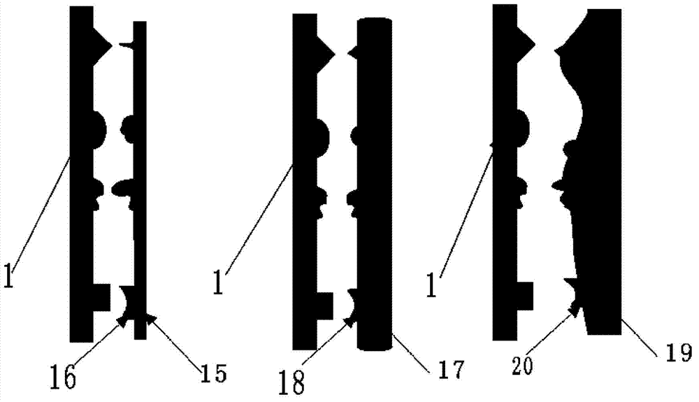
[0105] Based on the micro-nano processing method disclosed in the first embodiment and the micro-nano processing device disclosed in the second embodiment. Since there are many kinds of micro-nano structure materials to be processed, this embodiment gives a specific example. In this embodiment, only depositing copper micro-nano structure graphics on a flat gold substrate is taken as an example. In addition, it should be noted that the production of micro-nano structures of other materials, by replacing the electrochemical solution and the electrode plate, according to the following specific operation methods, The same can be achieved.
[0106] The micro-nano processing based on this embodiment of the present invention is as Figure 5 As shown, wherein, the micro-nano structure 3 to be prepared is a deposited copper micro-nano structure, the electrochemical solution 8 is a copper plating solution, an electrode plate 1, a substrate 2, a solution tank 9, a stirring device 10 and...
PUM
 Abstract
Description
Claims
Application Information
 - R&D
- Intellectual Property
- Life Sciences
- Materials
- Tech Scout
- Unparalleled Data Quality
- Higher Quality Content
- 60% Fewer Hallucinations
Browse by: Latest US Patents, China's latest patents, Technical Efficacy Thesaurus, Application Domain, Technology Topic, Popular Technical Reports.
© 2025 PatSnap. All rights reserved.Legal|Privacy policy|Modern Slavery Act Transparency Statement|Sitemap|About US| Contact US: help@patsnap.com