
Polycrystalline silicon ingot and its preparation method, polycrystalline silicon chip and crucible for polycrystalline silicon ingot casting

A polycrystalline silicon ingot and crucible technology, which is applied to the growth of polycrystalline materials, chemical instruments and methods, crystal growth, etc. Production, easy operation, high conversion efficiency

Active Publication Date: 2017-12-15
JIANGXI SAI WEI LDK SOLAR HI TECH CO LTD
View PDF6 Cites 0 Cited by
  • Summary
  • Abstract
  • Description
  • Claims
  • Application Information

AI Technical Summary

Problems solved by technology

Although the polycrystalline silicon ingot produced by this method has few initial dislocations and slow proliferation, it has the following disadvantages: (1) The crystal grains grow rapidly in the form of dendrites, and different dendrites are easy to squeeze each other, resulting in stress and defects; (2) The grown grains are relatively large, and once there are dislocations inside the large grains, it is easy to expand inside the entire large grains and occupy the entire grain; (3) The growth of dendrites exothermic, relatively The heat released by large grains during the growth process is likely to affect the supercooling required for the growth of other grains around them, making it difficult for other grains to grow, so this method is not suitable for large-scale industrial

Method used


Image

  • Polycrystalline silicon ingot and its preparation method, polycrystalline silicon chip and crucible for polycrystalline silicon ingot casting
  • Polycrystalline silicon ingot and its preparation method, polycrystalline silicon chip and crucible for polycrystalline silicon ingot casting
  • Polycrystalline silicon ingot and its preparation method, polycrystalline silicon chip and crucible for polycrystalline silicon ingot casting

Examples


Embodiment 1

[0043] The preparation method of polycrystalline silicon ingot comprises the following steps:

[0044] (1) A nucleation source is arranged at the bottom of the crucible to form a nucleation source layer;

[0045] Among them, the nucleation source is set at the bottom of the crucible: use a mixture of silicon powder and silicon nitride powder totaling 300g, wherein the mass ratio of silicon powder and silicon nitride powder is 6:4, with 500ml of alcohol, brush on the bottom of the crucible Coated and baked in a crucible oven at 800 degrees for 2 hours. The particle size of the silicon powder is 10um, and the particle size of the silicon nitride powder is 0.5-50um.

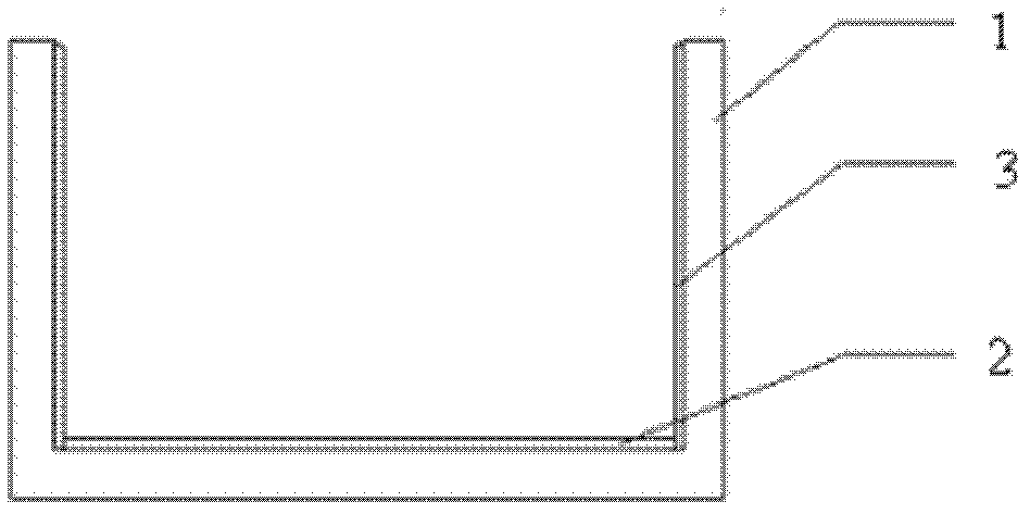
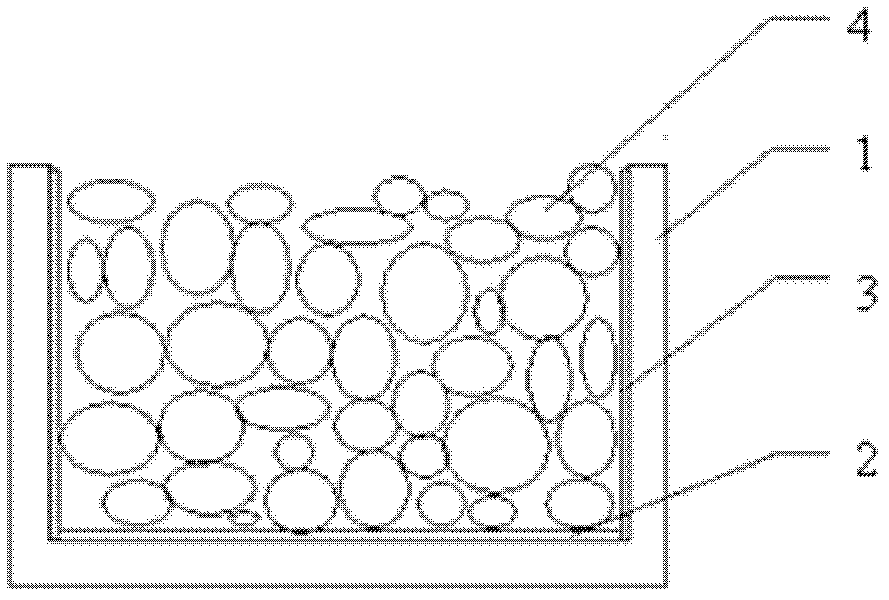
[0046] figure 1 It is a schematic diagram of the crucible for polycrystalline silicon ingot prepared in Example 1 of the present invention. Wherein, 1 is the crucible body, 2 is the nucleation source layer, and 3 is the silicon nitride layer coated on the side wall of the crucible.

[0047] (2) setting molten si...

Embodiment 2

[0056] The preparation method of polycrystalline silicon ingot comprises the following steps:

[0057] (1) A nucleation source is arranged at the bottom of the crucible to form a nucleation source layer;

[0058] Among them, the nucleation source is set at the bottom of the crucible: a total of 200g of a mixture of silicon carbide and silicon nitride powder is used, wherein the mass ratio of silicon carbide and silicon nitride powder is 8:2, with 500ml of water, using a compressed air spray gun, spraying On the bottom of the crucible, bake in a 1000 degree crucible oven for 2 hours. The particle size of silicon carbide and silicon nitride powder is 20um.

[0059] (2) setting molten silicon material on the nucleation source layer;

[0060] Among them, setting the molten silicon material on the nucleation source layer is as follows: 450-800 kg of solid silicon material is loaded above the nucleation source layer, and the crucible is heated to 1560 ° C to melt the solid silicon...

Embodiment 3

[0066] The preparation method of polycrystalline silicon ingot comprises the following steps:

[0067] (1) A nucleation source is arranged at the bottom of the crucible to form a nucleation source layer;

[0068] Among them, the nucleation source is set at the bottom of the crucible: use a mixture of carbon powder and silicon nitride powder totaling 300g, wherein the mass ratio of silicon carbide and silicon nitride powder is 6:4, with 500ml of alcohol, brush on the bottom of the crucible Coated and baked in a crucible oven at 800 degrees for 2 hours. The particle size of the carbon powder is 20um, and the particle size of the silicon nitride powder is 5um.

[0069] (2) setting molten silicon material on the nucleation source layer;

[0070] Among them, setting the silicon material in molten state on the nucleation source layer is: heating 450-800 kg of solid silicon material in another crucible to 1560 ° C to obtain molten silicon material, and casting the molten silicon ma...


PUM

PropertyMeasurementUnit
particle diameteraaaaaaaaaa

Abstract

The invention provides a method for preparing a polycrystalline silicon ingot, comprising the following steps: setting a nucleation source at the bottom of a crucible to form a nucleation source layer; setting molten silicon material on the nucleation source layer; controlling the temperature in the crucible A temperature gradient is formed by gradually rising in a direction perpendicular to the bottom of the crucible, so that the silicon material in the molten state is nucleated and crystallized by the nucleation source to produce a polycrystalline silicon ingot. The invention also provides a high-quality polysilicon ingot obtained by the preparation method, a polysilicon slice and a crucible for polysilicon ingot prepared by using the polysilicon ingot. The polycrystalline silicon ingot prepared by the preparation method has uniform and regular crystal grains, low dislocation density and no obvious dendrites and twins.

Description

technical field [0001] The invention relates to the field of polycrystalline silicon ingots, in particular to polycrystalline silicon ingots and a preparation method thereof, polycrystalline silicon slices and a crucible for polycrystalline silicon ingots. Background technique [0002] At present, the preparation method of polycrystalline silicon ingot mainly adopts the directional solidification system method (DSS for short) furnace crystal growth technology provided by GT Solar, which usually includes the steps of heating, melting, solidification growth, annealing and cooling. During the process of solidification and crystal growth, with the continuous cooling of the bottom of the crucible, the silicon material in molten state spontaneously forms random nucleation and the random nucleation gradually grows. However, since the initial nucleation is not controlled, dislocations are prone to occur during the nucleation process, resulting in irregular crystal orientation, irreg...

Claims


Application Information

Patent Timeline
Patent Type & Authority Patents(China)
IPC IPC(8): C30B28/06C30B29/06
Inventor 胡动力何亮雷琦钟德京张涛万跃鹏
Owner JIANGXI SAI WEI LDK SOLAR HI TECH CO LTD
Learn More