Power diode device and preparation method thereof

A technology for power diodes and devices is applied in the field of power diode devices and their preparation to achieve the effects of improving reverse voltage withstand capability, optimizing depth, width and spacing.

Active Publication Date: 2014-08-06
JIANGSU CORENERGY SEMICON CO LTD
View PDF3 Cites 3 Cited by
  • Summary
  • Abstract
  • Description
  • Claims
  • Application Information

AI Technical Summary

Problems solved by technology

In the traditional silicon device process, the lattice damage caused by ion implantation can be completely removed only by thermal annealing (generally at a temperature of about 1100 degrees); It is possible to remove the lattice damage caused by ion implantation only with a high degree of heat treatment
The heat treatment at 1500 degrees can decompose the GaN material on the surface of the device, reduce the Schottky barrier, increase the reverse leakage current of the Schottky electrode and reduce the reverse withstand voltage of the device; at the same time, heat treatment above 1500 degrees The requirements for annealing equipment are also very high, resulting in a substantial increase in device manufacturing costs
[0009] In summary, the traditional ion implantation field limiting ring process cannot be simply copied to the manufacturing process of power diode devices

Method used


Image

  • Power diode device and preparation method thereof
  • Power diode device and preparation method thereof
  • Power diode device and preparation method thereof

Examples


Embodiment Construction

[0055] The preferred embodiments of the present invention will be described in detail below in conjunction with the accompanying drawings, so that the advantages and features of the present invention can be more easily understood by those skilled in the art, so as to define the protection scope of the present invention more clearly.

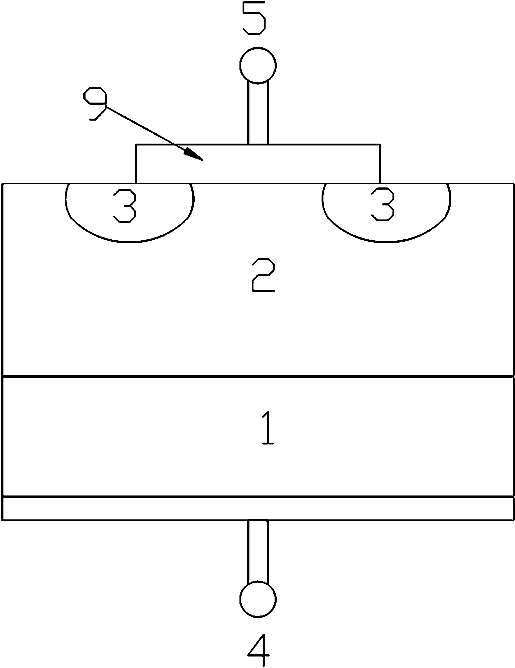
[0056] In an embodiment of the present invention: a power diode device, which includes a substrate 1, a buffer layer 6, an epitaxial layer 2, an ALN ​​layer 11, a field limiting ring 3, and an annular field plate 9 that are stacked to form a Schottky junction. The metal layer 10, the epitaxial layer 2 is electrically connected to the cathode 4, and the metal layer 10 is connected to the anode 5.

[0057] The epitaxial layer 2 is electrically connected to the cathode 4 , and the metal layer 10 is connected to the anode 5 .

[0058] as attached image 3 and 4 As shown, when the substrate 1 is a conductor, the cathode 4 can be arranged on...


PUM


Abstract

The invention discloses a power diode device, which comprises a stacked substrate, a buffer layer, an epitaxial layer, an ALN ​​layer, a field limiting ring, an annular field plate, and a metal layer forming a Schottky junction. The epitaxial layer and the metal layer form a Schottky junction The cathode is electrically connected, and the metal layer is connected to the anode. A plurality of annular concave-convex portions are formed on the annular field plate, the highest point of the convex portion of the annular field plate gradually rises from the inner side to the outer side of the power component, and the lowest point of the annular field plate gradually rises from the inner side to the outer side of the power component. Elevated, the projection of the annular field plate closest to the center of the power diode device to the epitaxial layer is located in the field limiting ring closest to the center, and the metal layer covers the recess of any annular field plate.

Description

technical field [0001] The invention relates to a power diode device and a preparation method thereof. Background technique [0002] For power diode devices to be able to withstand high voltages, advanced terminal structure designs must be used in the device structure. Its structure is as attached figure 1 As shown, the function of this terminal structure is to weaken the electric field enhancement peak at the edge of the electrode, flatten the electric field distribution, and avoid premature breakdown of the device. Therefore, in the design process of high-power Schottky devices, after determining the doping concentration and thickness of the voltage blocking layer, the design of the terminal structure around the Schottky electrodes will determine whether the device can withstand the required high voltage. [0003] The guard ring is the most commonly used terminal structure for power diode devices. Its manufacturing process is very mature for silicon-based devices. As sho...

Claims


Application Information

Patent Timeline
Patent Type & Authority Patents(China)
IPC IPC(8): H01L29/872H01L29/06H01L21/329
Inventor 朱廷刚
Owner JIANGSU CORENERGY SEMICON CO LTD
Why Eureka
Try Eureka