Fabricating method of GaN-based light-emitting component with vertical structure

A gallium nitride-based, light-emitting element technology, applied to electrical components, semiconductor devices, circuits, etc., can solve problems such as low process yield

Inactive Publication Date: 2012-11-14
ANHUI SANAN OPTOELECTRONICS CO LTD
View PDF4 Cites 8 Cited by
  • Summary
  • Abstract
  • Description
  • Claims
  • Application Information

AI Technical Summary

Problems solved by technology

Using this method to form an isolation region can simplify the overall manufacturing process, and can effectivel

Method used


Image

  • Fabricating method of GaN-based light-emitting component with vertical structure
  • Fabricating method of GaN-based light-emitting component with vertical structure
  • Fabricating method of GaN-based light-emitting component with vertical structure

Examples


Embodiment Construction

[0022] The implementation of the present invention will be described in detail below in conjunction with the accompanying drawings and examples, so as to fully understand and implement the process of how to apply technical means to solve technical problems and achieve technical effects in the present invention. It should be noted that, as long as there is no conflict, each embodiment and each feature in each embodiment of the present invention can be combined with each other, and the formed technical solutions are all within the protection scope of the present invention.

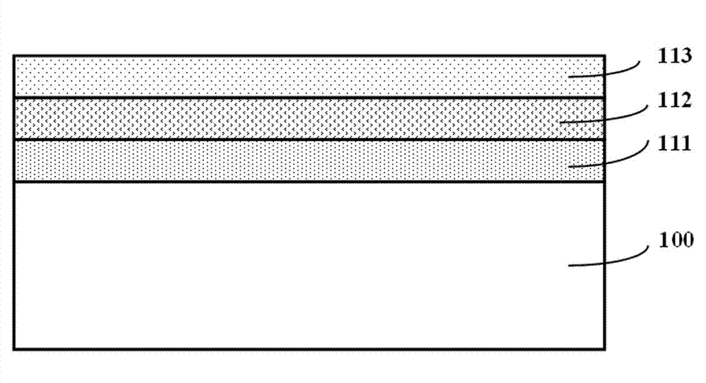
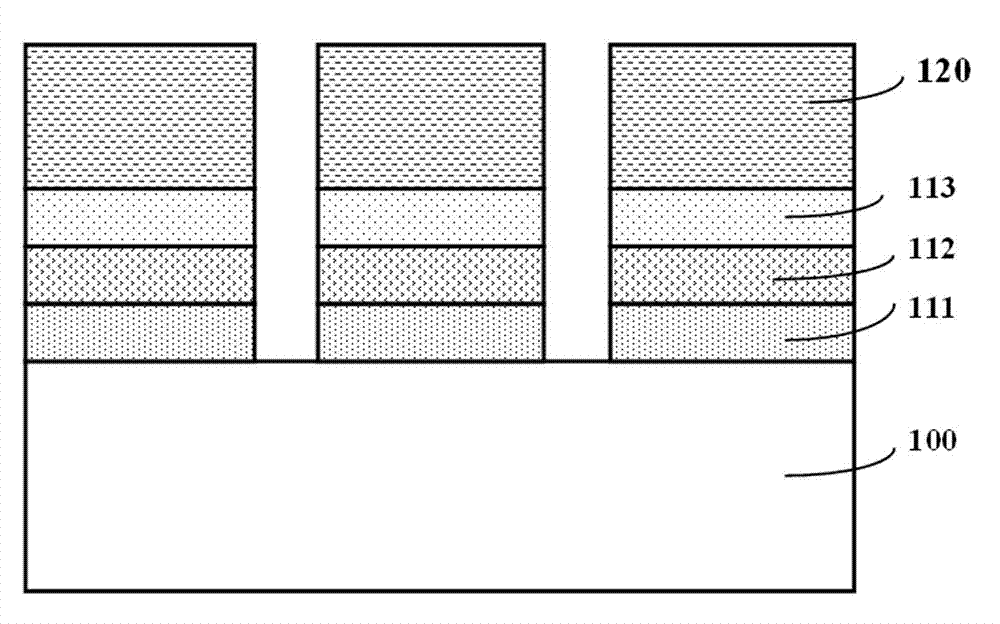
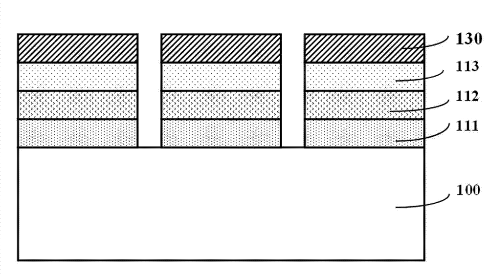
[0023] A method for manufacturing a gallium nitride-based light-emitting element with a vertical structure, the specific steps of which are as follows:

[0024] Such as Figure 7 As shown, a temporary substrate 200 is provided on which a GaN-based light-emitting epitaxial layer is epitaxially grown. It includes sequentially epitaxially growing an n-type layer 211 , a multi-quantum well (MQW) light-emitting ...


PUM

PropertyMeasurementUnit
Widthaaaaaaaaaa

Abstract

The invention discloses a fabricating method of a GaN-based light-emitting component with a vertical structure, which includes the steps of: providing a temporary substrate, growing a GaN-based light emitting epitaxial layer on the substrate, wherein the GaN-based light emitting epitaxial layer includes, from bottom to top, an n-shaped layer, a light emitting layer and a p-shaped layer; forming an insulated region on the light emitting epitaxial layer, and passivating and insulating the light emitting epitaxial layer of the insulated region through an ion injection method; sequentially forming a metallic reflector and a metal bonding layer on the light emitting epitaxial layer; providing a conductive substrate and bonding the conductive substrate with the light emitting epitaxial layer on the temporary substrate; removing the temporary substrate to expose the surface of the light emitting epitaxial layer; forming cutting lines on the exposed surface of the light emitting epitaxial layer, wherein the cutting lines are located inside the insulated region; dividing the light emitting epitaxial layer into a series of units along the cutting lines by using a laser scriber; and cleaving the backside of the conductive substrate to form chip granules.

Description

technical field [0001] The invention relates to a method for manufacturing a semiconductor light-emitting element, more specifically a method for manufacturing a gallium nitride-based light-emitting element with a vertical structure. Background technique [0002] In recent years, in order to improve the luminous power and efficiency of gallium nitride (GaN)-based light-emitting diodes, on the basis of traditional horizontal structure GaN-based light-emitting diode chip technology, a vertical structure GaN-based light-emitting diode chip technology based on substrate transfer has been developed. For example, a GaN-based light-emitting epitaxial layer is epitaxially deposited on a sapphire substrate, and then the light-emitting epitaxial layer is bonded or bonded to a semiconductor substrate or a metal substrate by wafer bonding or electroplating technology, and then the sapphire substrate is peeled off, polished or Removed by etching. In this way, on the one hand, the reflec...

Claims


Application Information

Patent Timeline
IPC IPC(8): H01L33/00
CPCH01L33/0075H01L33/32H01L33/20
Inventor 黄少华曾晓强吴志强
Owner ANHUI SANAN OPTOELECTRONICS CO LTD
Why Eureka
Try Eureka