Optical element, light-source apparatus, and projection-type display apparatus
A technology of optical components and light source devices, applied in the field of optical components
- Summary
- Abstract
- Description
- Claims
- Application Information
AI Technical Summary
Problems solved by technology
Method used
Image
Examples
no. 1 example )
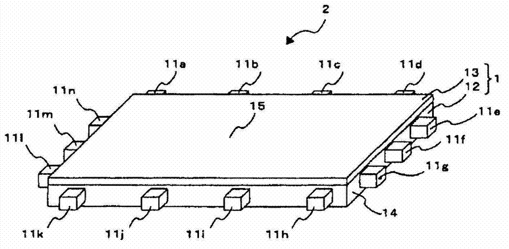
[0058] image 3 is a schematic diagram showing the configuration of the light source device according to the first embodiment. Figure 4 is an exemplary cross-sectional view showing the behavior of light in the light source device according to the present embodiment. In a light source device, each layer actually has a very large thickness, and there is a large difference in thickness between these layers. It is therefore difficult to draw the exact dimensions and proportions of these layers. Accordingly, in the drawings, the layers are not drawn to true scale and are therefore shown schematically.
[0059] Such as image 3 and Figure 4 As shown, the light source device 2 according to the present embodiment includes a plurality of light emitting elements 11 ( 11 a to 11 n ), and an optical element 1 into which light output from the light emitting elements 11 enters. The optical element 1 includes a light guide 12 and a directional control layer 13 , the light output from ...
no. 2 example )
[0100] For the wave vector conversion layer 18 , instead of a photonic crystal, a configuration in which a microlens array is arranged or a configuration using a layer with a rough surface may be used. Figure 7 is a perspective view schematically showing the direction control layer included in the light source device according to the second embodiment.
[0101] Such as Figure 7 As shown, in the direction control layer 23 , the wave vector conversion layer 28 including a microlens array is arranged on the surface of the plasmon excitation layer 17 . Even in the configuration including the wave vector conversion layer 28 including the microlens array, the direction control layer 23 can provide the same effect as the configuration including the wave vector conversion layer 18 composed of photonic crystals.
[0102] Figure 8A and Figure 8B is an exemplary cross-sectional view showing a manufacturing process of a configuration in which a microlens array is stacked on plasmon...
no. 3 example )
[0107] Figure 9 is a perspective view showing a direction control layer included in a light source device according to a third embodiment. Such as Figure 9 As shown, in the direction control layer 33 according to the third embodiment, the carrier generation layer 16, the plasmon excitation layer 17, the dielectric constant layer 19, and the wave vector conversion layer 18 are stacked on the light guide 12 in order.
[0108] Therefore, the third embodiment differs from the first embodiment in that dielectric constant layer 19 is independently arranged between plasmon excitation layer 17 and wave vector conversion layer 18 . The dielectric constant layer 19 has a dielectric constant set lower than that of the dielectric constant layer 20 (high dielectric constant layer 20 ) in the fourth embodiment described below, and is therefore called a low dielectric constant layer 19. Regarding the dielectric constant of low dielectric constant layer 19 , a range is allowed in which the...
PUM
 Abstract
Description
Claims
Application Information


