Array substrate cross curve repairing method, array substrate and liquid crystal display

A technology of an array substrate and a repair method, which is applied in the field of liquid crystal display manufacturing technology and can solve problems such as array substrate scrapping

Active Publication Date: 2012-11-28
BOE TECH GRP CO LTD
View PDF5 Cites 11 Cited by
  • Summary
  • Abstract
  • Description
  • Claims
  • Application Information

AI Technical Summary

Problems solved by technology

[0004] The object of the present invention is to solve the problem in the prior art that the crosshairs generated by the short circuit of the data line and the gate line on the arr

Method used


Image

  • Array substrate cross curve repairing method, array substrate and liquid crystal display
  • Array substrate cross curve repairing method, array substrate and liquid crystal display
  • Array substrate cross curve repairing method, array substrate and liquid crystal display

Examples


Embodiment Construction

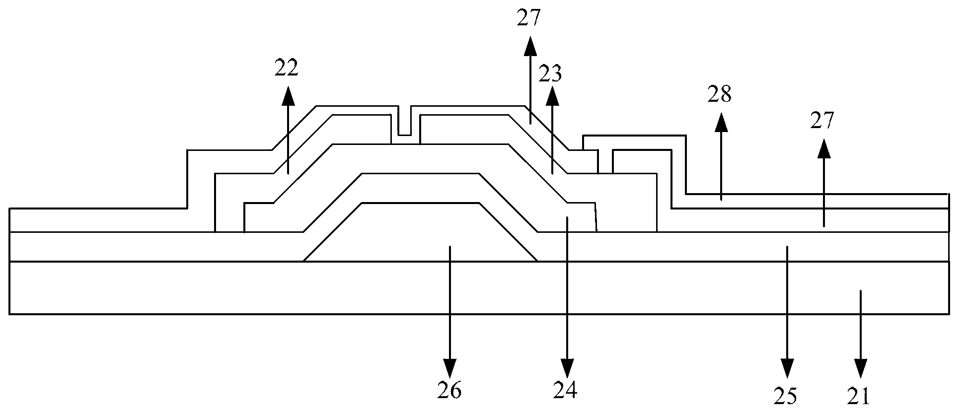
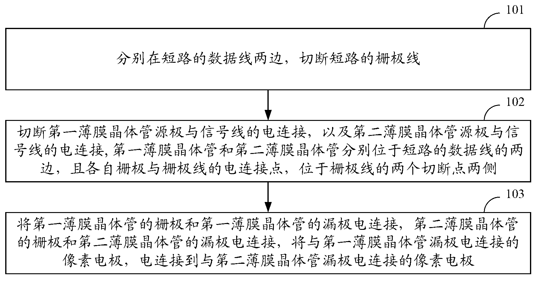
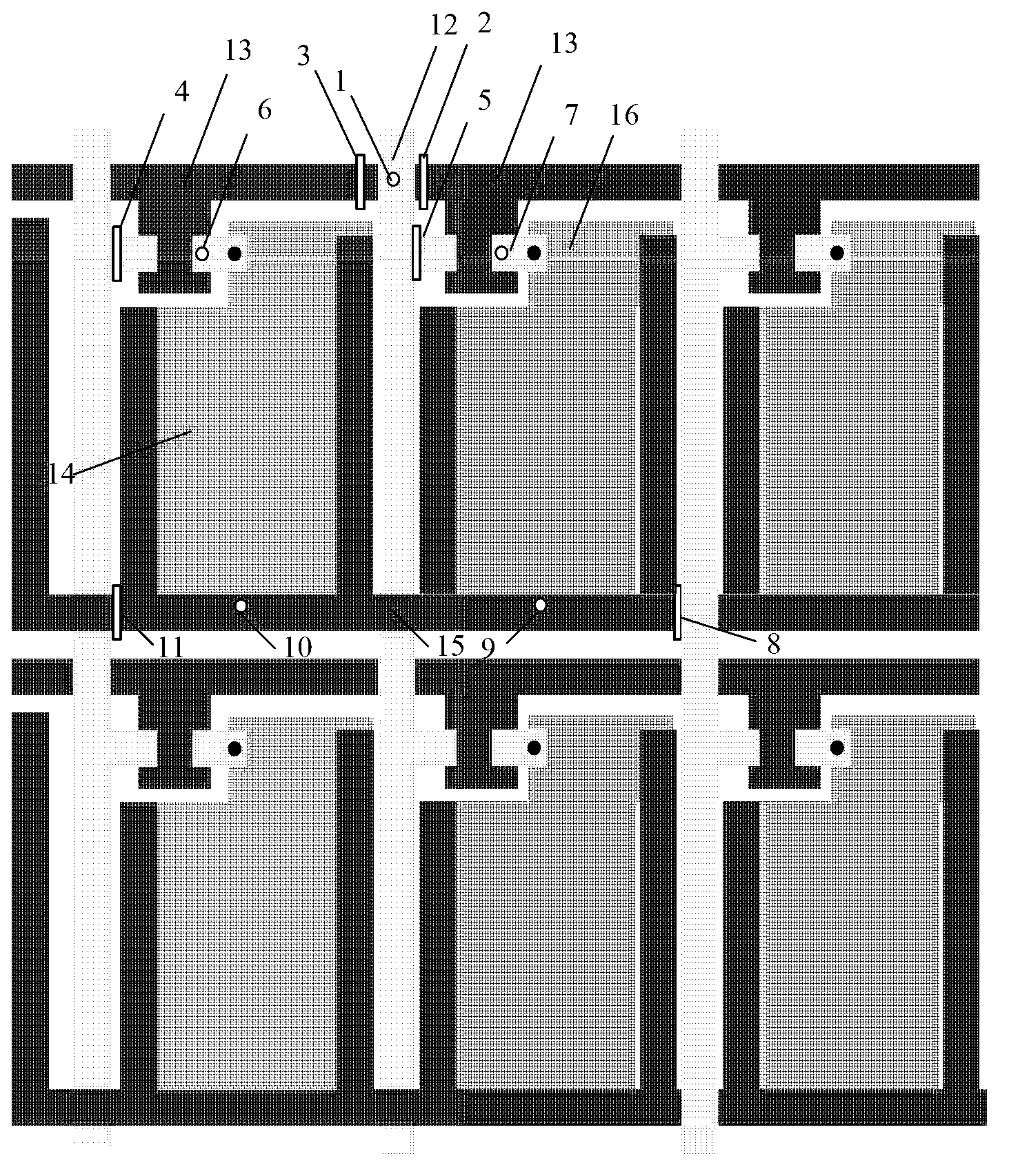
[0026] The present invention will be described below in conjunction with the embodiments and the accompanying drawings. In order to solve the problem that the array substrate is scrapped due to the crosshairs generated by the short circuit of the data line and the gate line on the array substrate in the prior art, the embodiment of the present invention provides A method for repairing crosshairs on an array substrate, which is used to repair the crosshairs generated by the short circuit of the data lines and gate lines on the array substrate, the data lines and the gate lines on the substrate, and the sources of the thin film transistors on the array substrate respectively. The electrode 22 is electrically connected to the gate 26, and the drain 23 of the thin film transistor is electrically connected to the pixel electrode 28, such as figure 2 shown, including the following steps:

[0027] Step 101 , respectively cut off the gate lines connected to the short-circuited data l...


PUM


Abstract

The invention provides an array substrate cross curve repairing method, an array substrate and a liquid crystal display, relating to the field of preparation processes of liquid crystal display screens and solving the problem of scrapped array substrate caused by cross curves generated by a data line and a grid line on the array substrate. The array substrate cross curve repairing method comprises the steps of: respectively cutting off the short-circuited grid line on two sides of the short-circuited data line, cutting off the connection between source electrodes of a first thin film transistor and a second thin film transistor and the data line, wherein the first thin film transistor and the second thin film transistor are respectively arranged on two sides of the short-circuited data line, electric connection points of grid electrodes of the first thin film transistor and the second thin film transistor and the grid line are respectively positioned on two sides of two cutting off points; and respectively electrically connecting the grid electrodes of the first thin film transistor and the second thin film transistor with respective drain electrodes, electrically connecting pixel electrodes electrically connected with the two drain electrodes, and because the short-circuited position of the grid line and the data line is firstly cut off when poor conditions happen, constructing a new path according to the pixel electrodes for connecting the grid line so that the cross curves are repaired.

Description

technical field [0001] The invention relates to the field of preparation technology of liquid crystal displays, in particular to a method for repairing cross lines on an array substrate, an array substrate and a liquid crystal display. Background technique [0002] A thin film transistor (Thin Film Transistor, TFT) generally refers to an insulated gate field effect transistor made of semiconductor thin film materials. This device usually consists of a semiconductor thin film and an insulating layer in contact with one side of the surface, and has a gate electrode, a source electrode and a drain electrode. TFTs are set on the array substrate, the Array substrate such as figure 1 As shown, it includes a supporting substrate 21 as a substrate, and the substrate 21 is composed of a conductive gate 26, a source 22 and a drain 23, an electrically insulating gate dielectric layer 25 and a semiconductive layer 24, and is electrically insulated. The gate dielectric layer 25 separat...

Claims


Application Information

Patent Timeline
IPC IPC(8): G02F1/13G02F1/1362G02F1/1368H01L21/77
Inventor 刘超张玉军赵德江杨维
Owner BOE TECH GRP CO LTD
Why Eureka
Try Eureka