

Method for manufacturing disposable RFID (Radio Frequency Identification) tag
An RFID tag, a one-time technology, applied to record carriers, antenna supports/installation devices, instruments, etc. used in machines, it can solve the problem of inconvenient direct production of RFID tag antennas, and achieve ultra-thin antenna thickness, process saving, suitable for wide range of effects
- Summary
- Abstract
- Description
- Claims
- Application Information
AI Technical Summary
Problems solved by technology
Method used
Image

Examples
Embodiment approach 1
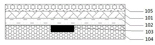
[0027] like Figure 4 As shown, the labels from top to bottom are: 105 surface graphic layer, 101 fragile layer, 102 antenna circuit layer, 103 chip layer, 106 self-adhesive layer, 107 bottom paper layer.
[0028] The production process is as follows: the first step is to hot stamp or cold transfer the antenna layer 102 on one side of the fragile layer 101; the second step is to package the chip layer 103 on the antenna layer 102; Type base paper layer 107 compound, the 4th step prints or prints graphic layer 105 as required on the other side of fragile layer. The fifth step is to cut and shape according to the shape of the label.
[0029] The graphic layer 105 can also be implemented first, that is, the graphic layer 105 is printed or printed on the destructible layer in advance, and then the antenna layer 102 is hot-stamped or cold-transferred on the other side of the destructible layer.
[0030] When in use, the RFID label is peeled off from the backing paper layer 107, a...
Embodiment approach 2
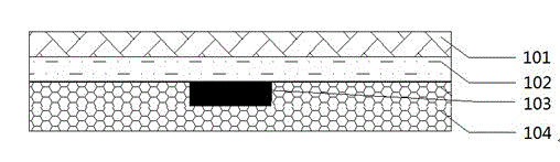
[0032] like Figure 5 As shown, the labels from top to bottom are: 105 surface graphic layer, 104 protective layer, 103 chip layer, 102 antenna circuit layer, 101 fragile layer, 106 self-adhesive layer, 107 bottom paper layer.
[0033] The manufacturing process is as follows: the first step is to combine the fragile layer 101 with the bottom paper layer 107 with the self-adhesive layer 106 . The second step is hot stamping or cold transfer antenna layer 102 on the fragile layer 101, the third step is to package the chip layer 103 on the antenna layer 102, the fourth step is to load the protective layer 104 on the antenna layer 102 and the chip layer 103, and the fifth step The first step is to print or print the graphic layer 105 on the protective layer 104 as required.
[0034] When in use, the RFID label is peeled off from the backing paper layer 107, and the entire label can be pasted on the commodity (item).
PUM
 Abstract
Description
Claims
Application Information