

Three-dimensional spiral inductor and forming method thereof
A spiral inductance, three-dimensional technology, applied in the direction of inductors, fixed inductors, fixed signal inductors, etc., can solve the problems of the large area occupied by the plane spiral, the large area of the semiconductor substrate, and the low Q value, so as to improve the Q value, The effect of reducing energy consumption and reducing the amount of current
- Summary
- Abstract
- Description
- Claims
- Application Information
AI Technical Summary
Problems solved by technology
Method used
Image

Examples
Embodiment Construction
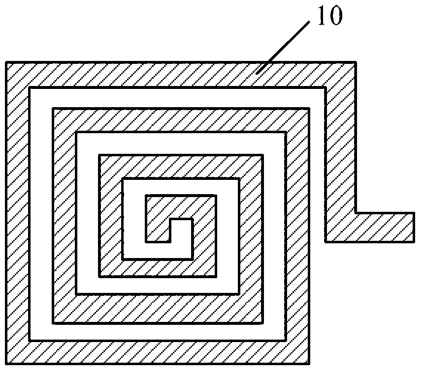
[0031] Since the inductance of the inductor is related to the number of turns of the inductor coil, the more the number of turns, the greater the inductance; the inductance of the inductor is also related to the area in the middle of the coil, and the larger the area in the middle of the coil, the greater the inductance. In the prior art, the inductors formed on the semiconductor substrate are mostly planar inductors, which are in the shape of a planar spiral. In order to increase the inductance of the inductor, the number of coil turns required for the inductor is large. Even if the multi-layer planar spiral inductors are stacked, The Q value of the inductor can be increased, but the area occupied by the inductor is still large, and because the middle area of each coil in the planar spiral coil is different, the middle area of the coil inside the inductor is very small, which is not conducive to increasing the inductance of the inductor.
[0032] To this end, the inventor ...
PUM
 Abstract
Description
Claims
Application Information