Light emitting diodes

A technology of light-emitting device and emission layer, applied in the field of white light LED, can solve the problems of color reproduction blue tone, LED failure, degradation of optical performance of emission layer, etc.

Inactive Publication Date: 2012-11-28
SEREN PHOTONICS
View PDF6 Cites 2 Cited by
  • Summary
  • Abstract
  • Description
  • Claims
  • Application Information

AI Technical Summary

Problems solved by technology

However, methods like this require ex situ deposition due to unused precursors
In addition, the deposition of such metal islands will lead to a substantial degradation of the optical properties of the emissive layer, which will eventually terminate the emission
In practice, this method degrades the lattice structure of the emissive layer and can eventually lead to failure of the LED
[0006] Second, there is a self-absorption problem in the current fabrication of phosphor-converted white LEDs
The intensity of blue light generally remains much higher than the yellow emission from wavelength converting materials, resulting in severe color reproduction problems as well as blue tinge in most existing white LEDs

Method used


Image

  • Light emitting diodes
  • Light emitting diodes
  • Light emitting diodes

Examples


Embodiment Construction

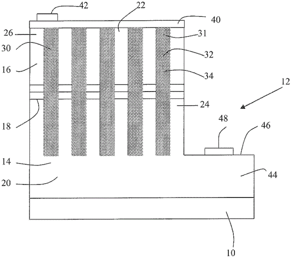
[0043] see figure 1 , a light-emitting device according to an embodiment of the invention comprises a substrate 10 , which in this case comprises a layer of sapphire, wherein a semiconductor diode system 12 is formed on the substrate 10 . Diode system 12 includes a lower layer 14 and an upper layer 16 with an emitter layer 18 therebetween. The lower layer 14 is an n-type layer formed of n-doped gallium nitride (n-GaN), and the upper layer 16 is a p-type layer formed of p-doped gallium nitride (p-GaN). The emissive layer in this embodiment is formed from In x Ga 1-x In of the N quantum well (QW) layer x Ga 1-x N and In forming the barrier layer y Ga 1-y N is formed (where x>y, x or y is from 0 to 1). These therefore provide multiple quantum wells within the emissive layer 18 . In another embodiment, there is a single In that forms a single emissive layer z Ga 1-z N layers (z from 0 to 1).

[0044]When electrical current is passed through semiconductor diode system 12...


PUM


Abstract

A light emitting device comprises first and second semiconductor layers (14,16) and an emitting layer (18) between the semiconductor layers (14,16), arranged to form a light emitting diode,-a gap (30) in one of the layers; and a metal (34) located in the gap (30) and near enough to the emitting layer (18) to permit surface plasmon coupling between the metal (34) and the emitting layer (18).

Description

technical field [0001] The present invention relates to light emitting diodes (LEDs), and more particularly to white LEDs, although it can also be used in LEDs of other colors. Background technique [0002] Due to the increasing energy shortage worldwide and the threat of global warming, the development of white solid-state lighting devices, mainly based on III-nitride blue LED chips with yellow phosphors, has become extremely important at present. Current commercial white light-emitting diodes (LEDs) are generally based on blue epitaxial wafers with high crystalline quality and are usually very expensive. This also makes such LEDs expensive and thus limits their use in general lighting. Therefore, there is a need to develop a new technology for manufacturing LEDs, especially white LEDs, which have higher luminous efficacy but have low prices that can be easily accepted by the market, thereby replacing conventional lighting sources. However, there are many challenges in or...

Claims


Application Information

Patent Timeline
Patent Type & Authority Applications(China)
IPC IPC(8): H01L33/50H01L33/20
CPCH01L33/508H01L33/08H01L33/20
Inventor T.王
Owner SEREN PHOTONICS
Why Eureka
Try Eureka