Class D audio power amplifier for noise suppression and audio signal processing method thereof

A technology for audio power and noise suppression, applied to amplifiers, amplifiers with semiconductor devices/discharge tubes, improved amplifiers to reduce noise effects, etc., can solve problems such as increased noise on and off switches, and reduce zero-crossing distortion and Effect of crosstalk noise and suppression of switching noise

Active Publication Date: 2012-12-05
JIAXING HEROIC ELECTRONICS TECH
View PDF4 Cites 13 Cited by
  • Summary
  • Abstract
  • Description
  • Claims
  • Application Information

AI Technical Summary

Problems solved by technology

However, this leads to an increase in the switching noise (POP and CLICK) of the improved Class D audio amplifier at the moment of power-on and power-off

Method used


Image

  • Class D audio power amplifier for noise suppression and audio signal processing method thereof
  • Class D audio power amplifier for noise suppression and audio signal processing method thereof
  • Class D audio power amplifier for noise suppression and audio signal processing method thereof

Examples


Embodiment 1

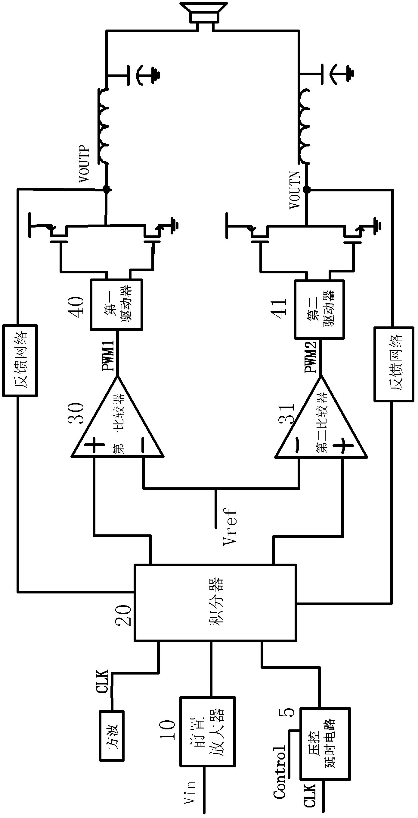
[0030] like image 3 As shown, according to a specific embodiment of the class D audio power amplifier of the present invention, the class D audio power amplifier includes an integrator 20, a comparator, a driver, a power switching element, and a feedback network. The class D audio power amplifier also includes a voltage-controlled delay circuit 5, which is used to control the delay of the signal so as to suppress the crosstalk noise and switching noise of the system.

[0031] The input terminal of the voltage-controlled time-delay circuit 5 inputs the square wave CLK as the reference wave, the control terminal control of the voltage-controlled time-delay circuit 5 inputs the control signal, and the output terminal of the voltage-controlled time-delay circuit 5 outputs a delayed square wave. Wave is a delayed square wave CLK. The square wave is input to the first reference wave input end of the integrator 20 , and the delayed square wave is input to the second reference wave ...

Embodiment 2

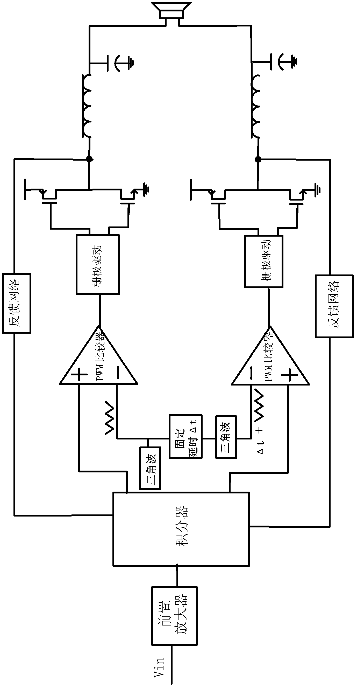
[0047] like Image 6 As shown, the circuit structure of this embodiment is basically the same as that of Embodiment 1, the difference is that the input terminal of the voltage-controlled delay circuit 5 inputs a triangular wave as a reference wave, and the control terminal control input of the voltage-controlled delay circuit 5 controls signal, the output end of the voltage-controlled delay circuit 5 outputs a delayed triangular wave, and the delayed triangular wave is a delayed triangular wave; the triangular wave is input to the inverting input of the first comparator 30, and the delayed square wave is input to the second comparator The inverting input end of 31; The first output end of integrator 20 is connected with the noninverting input end of first comparator 30, and the second output end of integrator 20 is connected with the noninverting input end of second comparator 31;

Embodiment 3

[0049] like Figure 7 As shown, the circuit structure of this embodiment is basically the same as that of Embodiment 1, the difference is that the input end of the voltage-controlled delay circuit 5 is connected to the output end of the first comparator 30, and the control of the voltage-controlled delay circuit 5 The control signal is input to the terminal control, the output terminal of the voltage-controlled delay circuit 5 is connected to the input terminal of the first driver 40 ; the output terminal of the second comparator 31 is connected to the input terminal of the second driver 41 .


PUM


Abstract

The invention discloses a class D audio power amplifier for noise suppression and an audio signal processing method thereof. The class D audio power amplifier at least comprises an integrator, a comparer, a driver, a power switch element, a feedback network and a voltage-controlled time-delay circuit, wherein the voltage-controlled time-delay circuit is used for controlling time delay of signals. Because the voltage-controlled time-delay circuit is additionally arranged, zero-crossing distortion and crosstalk noise of the class D audio power amplifier are reduced, the on-off noise (POP and CLICK) is lowered, and the THD+N (Total Harmonic Distortion + Noise) parameters are decreased. According to the invention, because a square wave modulation signal is used as a carrier signal of an audio input signal, a triangular wave generation circuit of the class D audio power amplifier of the prior art is omitted, a chip area is saved and the chip manufacturing cost is saved.

Description

technical field [0001] The invention relates to the technical field of audio power amplification, in particular to a Class D audio power amplifier for suppressing noise and an audio signal processing method thereof. Background technique [0002] like figure 1 As shown, a Class D audio amplifier uses a high frequency square wave modulation carrying an audio input signal Vin to control a power switching element. The power switching element drives the load speaker to produce sound. The size of the power switching element used in the class D audio amplifier in the prior art is generally large, and the parasitic capacitance of the gate is also large due to the large size, resulting in a large distortion of the small audio input signal Vin. Or when the audio input signal Vin is zero, crosstalk noise is generated due to the simultaneous switching of the power switching elements. [0003] like figure 2 As shown, when the audio input signal Vin is zero, since the improved class-...

Claims


Application Information

Patent Timeline
Patent Type & Authority Applications(China)
IPC IPC(8): H03F3/217H03F1/26
Inventor 杨志飞黄武康代军赵玉月马琳沈世龙张伟周长胜殷明张林俊
Owner JIAXING HEROIC ELECTRONICS TECH
Why Eureka
Try Eureka