Class d audio power amplifier for suppressing noise and its audio signal processing method
A technology of audio power and amplifier, which is applied in the field of class D audio power amplifier and its audio signal processing, which can solve the problems of distortion, power supply noise aggravation, switch machine noise increase, etc., and achieve the effect of reducing zero-crossing distortion and crosstalk noise
- Summary
- Abstract
- Description
- Claims
- Application Information
AI Technical Summary
Problems solved by technology
Method used
Image
Examples
Embodiment 1
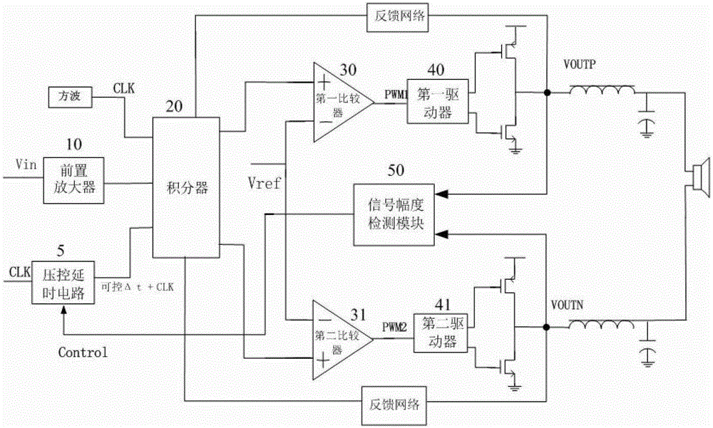
[0036] Such as image 3 As shown, according to a specific embodiment of the class D audio power amplifier of the present invention, the class D audio power amplifier includes an integrator 20, a comparator, a driver, a power switching element, and a feedback network. The class D audio power amplifier also includes a voltage-controlled delay circuit 5 for controlling signal delay so as to suppress system crosstalk noise and switching noise and a signal amplitude detection module 50 .
[0037] The input terminal input of the voltage-controlled delay circuit 5 is used as the square wave CLK of the reference wave, and the control terminal of the voltage-controlled delay circuit 5 inputs the control control signal. The control signal of the voltage-controlled delay circuit 5 can be a switch enabling signal, a signal Amplitude identification signal or enabling control signal in other systems. In this embodiment, the control signal of the voltage-controlled delay circuit 5 uses a si...
Embodiment 2
[0061] Such as Image 6 As shown, the circuit structure of this embodiment is basically the same as that of Embodiment 1, the difference is that the input terminal of the voltage-controlled delay circuit 5 inputs a triangular wave as a reference wave, and the control terminal control input of the voltage-controlled delay circuit 5 is input by The control signal of the signal amplitude detection module output, the output end of the voltage-controlled delay circuit 5 outputs a delayed triangular wave, and the delayed triangular wave is a delayed triangular wave; The square wave is input to the inverting input of the second comparator 31; the first output of the integrator 20 is connected to the non-inverting input of the first comparator 30, and the second output of the integrator 20 is connected to the non-inverting input of the second comparator 31. input connection;
Embodiment 3
[0063] Such as Figure 7 As shown, the circuit structure of this embodiment is basically the same as that of Embodiment 1, the difference is that the input end of the voltage-controlled delay circuit 5 is connected to the output end of the first comparator 30, and the control of the voltage-controlled delay circuit 5 Input the control signal output by the signal amplitude detection module, the output of the voltage-controlled delay circuit 5 is connected to the input of the first driver 40; the output of the second comparator 31 is connected to the input of the second driver 41.
PUM
 Abstract
Description
Claims
Application Information


