
Method for testing processing residual stress of 'through-silicon via'-Cu structure

A technology of residual stress and testing method, applied in the direction of force/torque/work measuring instrument, measuring device, mechanical device, etc., can solve the problems that the accuracy of test results needs to be improved, and the residual stress results are quite different, and the method is simple and reliable , the effect of accurate test results

Inactive Publication Date: 2012-12-12
BEIJING UNIV OF TECH
View PDF3 Cites 20 Cited by
  • Summary
  • Abstract
  • Description
  • Claims
  • Application Information

AI Technical Summary

Problems solved by technology

[0004] In the existing residual stress tests of TSV-Cu structures, methods such as nanoindentation, Raman spectroscopy, and X-rays are often used to test the residual stress of TSV, but the residual stress results of different methods are quite different. And different test methods will cut and split the sample, etc., which will release the residual stress in the sample, which makes the accuracy of the test results need to be improved

Method used


Image

  • Method for testing processing residual stress of 'through-silicon via'-Cu structure
  • Method for testing processing residual stress of 'through-silicon via'-Cu structure
  • Method for testing processing residual stress of 'through-silicon via'-Cu structure

Examples


Embodiment Construction

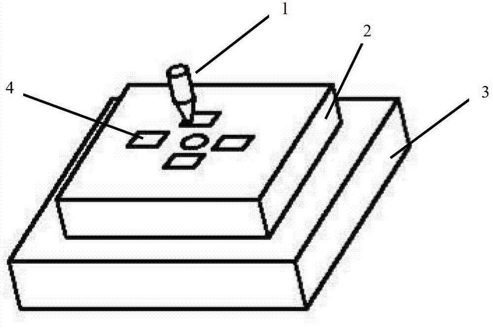
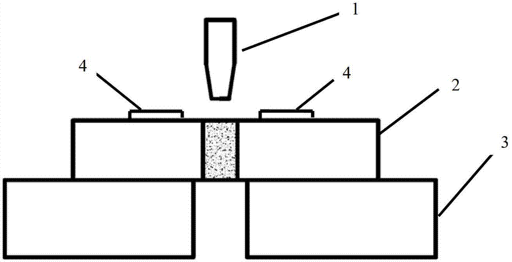
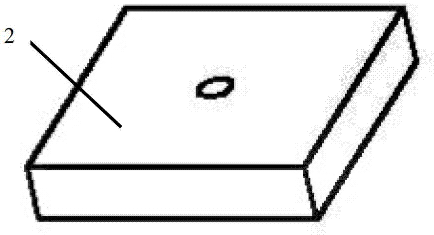
[0022] The experimental device is mainly composed of an indenter 1, an experimental sample 2, and a sample carrier 3. As shown in the attached picture. The experimental steps are as follows:

[0023] Firstly, the experimental sample 2 is placed on the sample carrier 3, the sample carrier 3 has a hole in the middle, and the diameter D of the hole is slightly larger than the diameter of TSV-Cu. Align the three parts of the indenter, TSV-Cu (copper-filled part) and the hole of the sample carrier 2.

[0024] Then, use the indenter 1 to slowly squeeze the copper downward, the loading speed is 0.1mm / min, and the diameter of the end of the indenter should be slightly smaller than the diameter of the TSV. During the loading process, the displacement and pressure values ​​were recorded, and the platinum electric heating plate 4 was used to heat the sample at the same time, with a loading accuracy of 1K, which promoted diffusion slip at the interface between copper and silicon. By ob...


PUM


Abstract

The invention discloses a method for testing processing residual stress of a 'through-silicon via'-Cu structure, and belongs to the technical field of electronic information. The method includes downwardly squeezing a copper cylinder in a through-silicon via in a test sample by a pressure head, simultaneously recording the displacement and the pressure F when the pressure head acts downwardly to obtain a pressure F and displacement curve and a threshold value of the pressure F when the pressure F is reduced, and substituting the threshold value of the pressure F in a pressure and interfacial shear stress conversion formula to obtain a shear stress threshold value tau 0 when a copper and silicon interface in the TSV-Cu structure manufactured by a copper plating process slips; and computing to obtain the to-be-measured residual stress of the 'through-silicon via' TSV-Cu structure via the shear stress threshold value tau 0. The method has the advantages that completeness of the test sample is kept to the greatest extent, operation, such as cutting the test sample, which affects release of the residual stress, is omitted, and a test result is accurate; and a residual stress computing method is simple and reliable, and the positive or negative property of the residual stress can be visually judged.

Description

technical field [0001] The present invention relates to a method for testing process residual stress, which is named "shear stress threshold method" in this patent. It is oriented to the next generation of three-dimensional (3D) interconnected electronic packaging technology. It has invented a new technology for the process residual stress generated in the manufacturing process of the "Through-Silicon Via" TSV (Through-Silicon Via) 3D interconnected packaging structure produced by the copper plating process. The invention relates to a residual stress test method for TSV-Cu (through-silicon via made by copper plating process) process based on interface shear stress, which belongs to the field of electronic information technology. Background technique [0002] With the rapid development of the information industry and the increasing consumer demand for smaller, more convenient, and higher reliability electronic products, traditional planar (2D) electronic packaging technology ...

Claims


Application Information

Patent Timeline
Patent Type & Authority Applications(China)
IPC IPC(8): G01N19/00G01L5/00
Inventor 秦飞武伟安彤夏国峰刘程艳于大全万里兮
Owner BEIJING UNIV OF TECH
Learn More