Integrated optical chip with high-frequency precompensation and high-speed optical communication device

A pre-compensation, optical chip technology, applied in the field of optical communication, can solve the problems of production scale expansion, high production cost, chip reduction, etc., and achieve the effect of easy mass production, low production cost, and compact size

Active Publication Date: 2012-12-12
SUZHOU CREALIGHTS TECH
View PDF9 Cites 2 Cited by
  • Summary
  • Abstract
  • Description
  • Claims
  • Application Information

AI Technical Summary

Problems solved by technology

However, in order to increase the speed / bandwidth of the optical chip, it is required to greatly reduce the capacitive reactance of the chip, including reducing the parasitic capacitance, etc., but this directly leads to the reduction of the size of the optical chip, which in turn requires a change in the corresponding process equipment requirements. At the same time, due to the smaller size of the optical chip, heat dissipation and crosstalk have also become technical problems.
[0004] The current solution adopted by the industry is to use expensive process equipment to produce high-speed optical chips / optical devices. Due to its high production cost, it directly limits the expansion of its production scale, resulting in low product yield.

Method used


Image

  • Integrated optical chip with high-frequency precompensation and high-speed optical communication device
  • Integrated optical chip with high-frequency precompensation and high-speed optical communication device
  • Integrated optical chip with high-frequency precompensation and high-speed optical communication device

Examples


Embodiment Construction

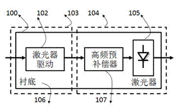
[0025] The invention discloses an integrated optical chip with high-frequency pre-compensation, including an optical chip, a high-frequency pre-compensator, and an optical chip driver, and a high-speed optical communication device that can be manufactured by using the integrated optical chip.

[0026] figure 1 Taking the laser application as an example, the integrated optical chip 100 with high-frequency pre-compensation is monolithically integrated or mixed integrated on the same substrate 106. The substrate 106 can be a silicon substrate, an indium phosphide substrate, or a ceramic substrate. Or other substrates based on different application needs. The laser 105 may be a distributed Bragg reflective semiconductor laser (DFB-LD), an electro-absorption modulated laser (EML) or other lasers, and the bandwidth of these lasers may be sufficiently high or relatively limited.

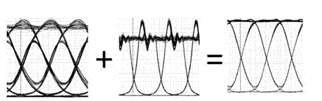
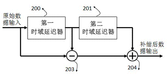
[0027] The signal transmission process is that when the electrical signal data enters the laser driver ...


PUM


Abstract

The invention discloses an integrated optical chip with high-frequency precompensation. The integrated optical chip is characterized in that active devices (such as a laser, an optical amplifier, a detector and a modulator) and an integrated circuit (IC) are integrated on a same substrate (such as a silicon substrate, an indium phosphide substrate or a ceramic substrate) in a single or hybrid manner. Based on different application backgrounds, an integrated high-frequency precompensation method can be realized by an active method, also can be realized by a passive method, so that the advantages similar to those of a large-scale integrated circuit such as low cost, small size, low power consumption, flexible expansion and high reliability can be achieved.

Description

technical field [0001] The invention relates to an integrated optical chip with high frequency pre-compensation, low cost, small size, low power consumption, flexible expansion and high reliability and a high-speed optical communication device with the optical chip, belonging to the field of optical communication. Background technique [0002] With the vigorous construction of cloud computing, mobile Internet, data centers, etc., the global market has an urgent and direct demand for bandwidth and broadband networks. At present, the optical communication network is developing in the direction of integration, low power consumption, intelligence and large capacity, while high-speed optical chips and their corresponding optical devices are highly integrated in function and size, as well as low cost, low power consumption and large capacity. The advantages of bandwidth, etc., can meet the growing requirements of data services, network resources, etc. [0003] In high-speed broad...

Claims


Application Information

Patent Timeline
Patent Type & Authority Applications(China)
IPC IPC(8): H04B10/00
Inventor 胡朝阳郑晓锋刘俊
Owner SUZHOU CREALIGHTS TECH
Why Eureka
Try Eureka