Method and device for measuring thickness of wafer

A technology of wafer thickness and measurement method, applied in the field of precision measurement, can solve the problems of affecting measurement accuracy, accuracy impact, and difficulty in unifying measurement data, and achieve the effects of convenient use, improved measurement accuracy, and high measurement accuracy

Inactive Publication Date: 2012-12-26
KUNSHAN YUNCO PRECISION IND TECH
View PDF6 Cites 9 Cited by
  • Summary
  • Abstract
  • Description
  • Claims
  • Application Information

AI Technical Summary

Problems solved by technology

In this measurement method, each point of the wafer will be subjected to gravity during the measurement process. For example, if the contact measurement method is used, the probe acts vertically downward on the surface of the wafer, just in the same direction as the gravity of each point on the surface, resulting in Downward force becomes greater, more likely to cause wafer fragmentation
As for the non-contact measurement method, due to the laser irradiation method for measurement, it will be difficult to unify the measurement data of each layer due to the different reflection effects of different measurement materials, especially for the measurement of the glass lay

Method used


Image

  • Method and device for measuring thickness of wafer

Examples


Embodiment Construction

[0020] The technical solutions of the present invention will be clearly and completely described below in conjunction with the accompanying drawings of the present invention. Apparently, the described embodiments are only some of the embodiments of the present invention, not all of them. Based on the embodiments of the present invention, all other embodiments obtained by persons of ordinary skill in the art without creative efforts fall within the protection scope of the present invention.

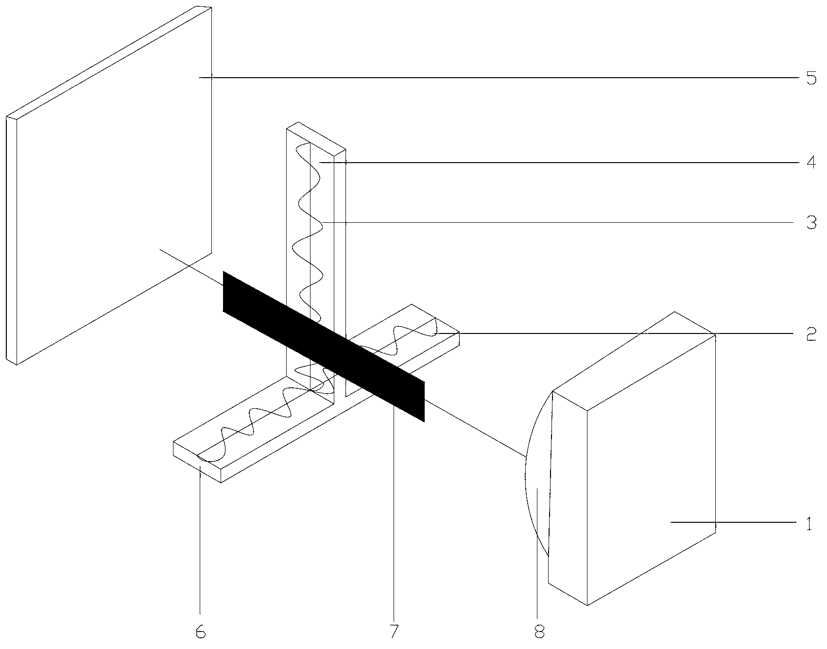
[0021] The wafer thickness measuring method of the embodiment of one aspect of the present invention is characterized in that the wafer is kept in a vertical state during the measurement process, and the vacuum chuck is also vertically arranged. Forced by gravity parallel to the wafer surface.

[0022] In one embodiment of the present invention, the wafer thickness measurement method adopts a touch probe with a horizontal layout, and the right probe of the touch probe moves from the horizo...


PUM


Abstract

The invention provides a method and a device for measuring thickness of a wafer. The method is characterized in that the wafer is kept in a vertical state during measurement and a vacuum chuck is also arranged vertically, so that the gravity of each point on the surface of the wafer is parallel to the surface of the wafer under the condition that the wafer is adsorbed. According to the invention, the problems of the surface damage and the surface fracture of the wafer easily caused by adopting a contact probe in the existing wafer for the vertical measurement, as well as the problems that the measurement accuracy of the non-contact measurement for transparent materials and surface high-brightness materials cannot meet market requirements and the like, are solved.

Description

technical field [0001] The invention relates to the technical field of precision measurement, in particular to a wafer thickness measurement method and device. Background technique [0002] As the core product in the solar energy field, the quality of wafers determines the rise and fall of the industry, and the processing and manufacturing technology and quality control standards around wafers are developing rapidly to meet the increasingly high performance requirements of the market. [0003] The wafer is a brittle sheet-like plate, generally composed of 4 layers of materials, the first layer is the wafer layer, the second layer is the adhesive, the third layer is the glass, and the fourth layer is the adhesive tape. The process is made into finished wafers, and then the next process is scribing, grooving and other processing. The thickness uniformity of the finished wafer will determine the processing quality of the subsequent process, and ultimately affect the performanc...

Claims


Application Information

Patent Timeline
IPC IPC(8): G01B11/06
Inventor 赵春花
Owner KUNSHAN YUNCO PRECISION IND TECH
Why Eureka
Try Eureka