Semiconductor memory, system, and method of operating semiconductor memory

An operation method and semiconductor technology, applied in static memory, digital memory information, information storage, etc., can solve the problem of increasing the dissipation power of semiconductor memory, and achieve the effect of reducing dissipation power and preventing fluctuations

Active Publication Date: 2013-01-02
FUJITSU SEMICON MEMORY SOLUTION LTD KANAGAWA
View PDF8 Cites 12 Cited by
  • Summary
  • Abstract
  • Description
  • Claims
  • Application Information

AI Technical Summary

Problems solved by technology

However, the multiple circuit blocks do not always operate at maximum power dissipation
If the power supply voltage generating capability of the voltage generating unit is too large, the power dissipation of the semiconductor memory increases

Method used


Image

  • Semiconductor memory, system, and method of operating semiconductor memory
  • Semiconductor memory, system, and method of operating semiconductor memory
  • Semiconductor memory, system, and method of operating semiconductor memory

Examples


Embodiment Construction

[0025] Embodiments will be described below with reference to the drawings. Signal wires that transmit signals are indicated by the same symbols as the signal names. Signals marked with a "Z" on the end are based on positive logic. Signals marked with a " / " at the top or an "X" at the end are based on negative logic. In the drawings, double square symbols represent external terminals. The external terminals are, for example, pads in the semiconductor chip or wires of a package covering the semiconductor chip. Signals provided via external terminals are indicated by the same symbols as the terminal names.

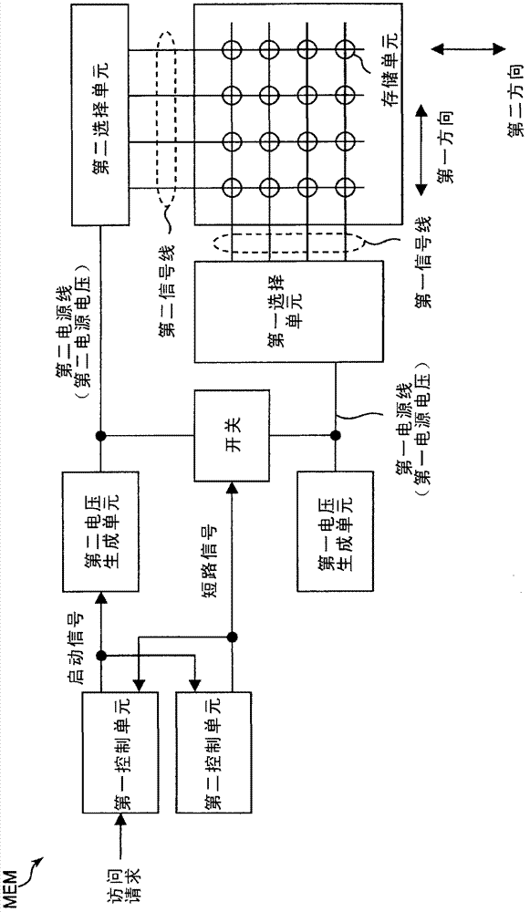
[0026] figure 1 The figure shows an example of a semiconductor memory in one embodiment. The semiconductor memory has a plurality of memory cells arranged in a matrix, a first control unit, a second control unit, a first voltage generation unit, a second voltage generation unit, switches, a first selection unit, and a second selection unit.

[0027] The first selection ...


PUM


Abstract

The invention discloses a semiconductor memory, a system, and a method of operating the semiconductor memory. A memory has memory cells in a matrix; a first selection unit selecting any of first signal lines in the memory cells, in response to an access request; a second selection unit selecting any of second signal lines in the memory cells, after the first selection unit starts operating; a first voltage generation unit generating a first power supply voltage supplied to the first selection unit; a second voltage generation unit generating a second power supply voltage supplied to the second selection unit, when a start-up signal is active; a switch short-circuiting first and second power supply lines, when a short-circuit signal is active; and a power supply voltage control unit which activates the start-up signal in response to the access request, activates the short-circuit signal after a predetermined time elapses since activation of the start-up signal, deactivates the short-circuit signal and the start-up signal after completion of access operations.

Description

technical field [0001] The present embodiment relates to a semiconductor memory having a low power consumption mode and a system in which the semiconductor memory is mounted. Background technique [0002] A method has been proposed by which, in a semiconductor memory such as a DRAM, if a row-related and a column-related circuit block are not operating, the supply of a power supply voltage to these circuit blocks is stopped, thereby reducing a leakage current flowing through a non-operating circuit block ( See, for example, Japanese Patent Application Laid-Open Nos. 2008-27547 and 2010-135047). There has also been proposed another method by which, in a DRAM, an operating frequency is identified based on a column address strobe (CAS) latency set in a mode register to change the generated internal power supply voltage using a voltage generating unit according to the identified operating frequency capability, thereby reducing power dissipation (for example, see Japanese Patent ...

Claims


Application Information

Patent Timeline
Patent Type & Authority Applications(China)
IPC IPC(8): G11C11/4074
CPCG11C11/4072G11C11/4074G11C11/40615G11C5/14
Inventor 佐藤贵彦
Owner FUJITSU SEMICON MEMORY SOLUTION LTD KANAGAWA
Why Eureka
Try Eureka