

Detector and detection method for wafer position
A detection device and detection method technology, applied in the direction of measuring devices, optical devices, semiconductor/solid-state device testing/measurement, etc., can solve the problem of affecting image data collection of camera components, inability to accurately detect wafers, secondary cleaning and drying processes Buried hidden dangers and other problems to achieve the effect of improving reliability
- Summary
- Abstract
- Description
- Claims
- Application Information
AI Technical Summary
Problems solved by technology
Method used
Image

Examples
Embodiment Construction
[0019] In order to describe the technical content, structural features, achieved goals and effects of the present invention in detail, the following will be described in detail in conjunction with the embodiments and accompanying drawings.
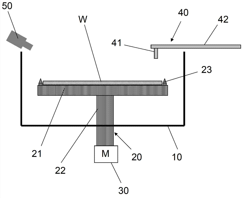
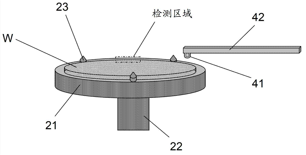
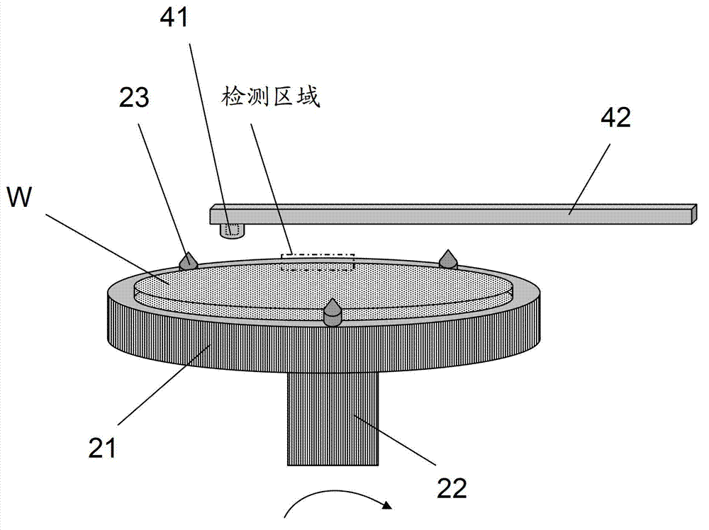
[0020] see figure 1 with figure 2 , is a schematic diagram of an embodiment of the wafer position detection device of the present invention. The wafer position detection device of the present invention includes a process chamber 10, a mounting table 20, a driving device 30, an air blowing device 40, a camera device 50 and an image processing device (not shown in the figure).
[0021] The process chamber 10 is used to perform corresponding processes on the wafer W, and in the present invention, the process chamber 10 may be used to perform wet cleaning and drying processes on the wafer W. The mounting table 20 has a circular carrying portion 21 for placing the wafer W and a supporting portion 22 whose one end is connected to the center o...
PUM
| Property | Measurement | Unit |
|---|---|---|
| Diameter | aaaaa | aaaaa |
Abstract
Description
Claims
Application Information