Admittance spectrum principle-theory method for researching performance of organic semiconductor

A technology of organic semiconductors and admittance spectroscopy, which is applied in the direction of single semiconductor device testing, measuring devices, instruments, etc., can solve the problems of complex operation, inability to accurately measure carrier mobility, measurement limitations, etc., and achieve simple test conditions and measurement The effect of expensive equipment and complicated operation

Inactive Publication Date: 2013-01-23
NANJING UNIV OF POSTS & TELECOMM
View PDF5 Cites 6 Cited by
  • Summary
  • Abstract
  • Description
  • Claims
  • Application Information

AI Technical Summary

Problems solved by technology

But it also has its own limitations: First, the TOF method has high requirements on the thickness of the organic layer, usually on the order of microns, which is very expensive for organic semiconductors, especially for many new materials, sometimes even in the synthesis technology. It is difficult to obtain enough samples; second, the thickness of the organic layer of the actual semiconductor device is generally at the nanometer level, which is very different from the thickness required by the TOF method, and the mobility measured by the TOF method cannot truly represent the migration of the actual organic semiconductor device. thirdly, TOF equipment is expensive, the operation is complicated, and the measurement is subject to many restrictions; fourthly, it has been reported in the literature that for some dispersive materials, the TOF method cannot accurately measure the carrier mobility

Method used


Image

  • Admittance spectrum principle-theory method for researching performance of organic semiconductor
  • Admittance spectrum principle-theory method for researching performance of organic semiconductor
  • Admittance spectrum principle-theory method for researching performance of organic semiconductor

Examples


Embodiment Construction

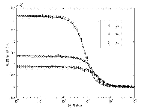
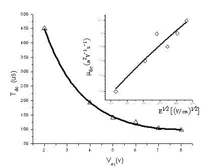
[0021] The invention proposes a method for studying the properties of organic semiconductors based on the admittance spectrum principle. Under small signal perturbation, based on space charge limited current theory SCLC, the theoretical admittance model of single carrier injection and no trap is established. Fitting the Capacitance of Organic Semiconductor Devices Using the Least Squares Principle , conductance , the imaginary part of the impedance or the real part of the impedance , resulting in the carrier migration time and the dispersion parameter of the organic layer semiconductor , , and then according to the formula get mobility .

[0022] Admittance model:

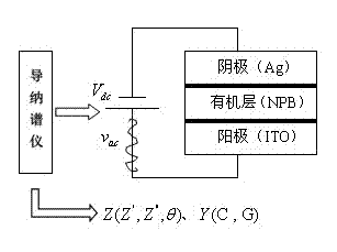
[0023] Consider a simple single-layer device such as figure 1 , between the anode and the cathode is the organic semiconductor to be tested, called the organic layer. In order to facilitate the establishment of the theoretical model, we make the following assumptions: first, the interface bet...


PUM


Abstract

The invention discloses an admittance spectrum theory-based method for researching performances of an organic semiconductor. The method comprises the following steps of: establishing a theoretical admittance model based on an SCLC (Spatial Charge Limiting Current) theory, see formula 1; fitting the capacitance, the conductance and the imaginary part or real part of the impedance of an organic semiconductor device by adopting a principle of least squares, so as to obtain the carrier mobility and the dispersion parameters of the organic semiconductor. The method has the advantages that firstly, the carrier mobility of the organic semiconductor in a real device is directly measured, so that the transportation performance of the organic semiconductor can be reflected truly; secondly, not only the carrier mobility of the organic semiconductor can be measured, but also the dispersion parameters which present the performances of the organic semiconductor can be measured; and thirdly, compared with a traditional TOF (Time of Flight) technique, the cots can be saved, for one reason, the TOF requires that the thickness of an organic semiconductor to be tested achieves the micron level, such is expensive in price for some materials, especially for new materials.

Description

technical field [0001] The invention relates to a method for studying the properties of organic semiconductors based on the admittance spectrum principle. The method can measure the carrier mobility and its dispersion parameter that characterize the transport performance of the organic semiconductor. technical background [0002] In recent years, organic semiconductor devices have developed rapidly and have attracted more and more attention, such as organic light-emitting diodes (OLEDs), organic solar cells (OPVs), and organic field-effect transistors (OFETs). The charge transport capability is one of the key factors affecting the device performance, and the carrier mobility is an important parameter to characterize the charge transport capability. By mastering the essential properties of carrier mobility, the required organic semiconductor materials can be synthesized according to different requirements, and the performance of organic semiconductor devices can be optimized...

Claims


Application Information

Patent Timeline
Patent Type & Authority Applications(China)
IPC IPC(8): G01R31/26G01N27/00
Inventor 唐超王徐亮刘瑞兰戎舟徐慧黄维
Owner NANJING UNIV OF POSTS & TELECOMM
Why Eureka
Try Eureka