A method of manufacturing a back-illuminated cmos image sensor

An image sensor and manufacturing method technology, applied in the field of image sensors, can solve the problem of high requirements for deep groove etching equipment, achieve the effects of reducing process complexity, achieving zero mismatch, and reducing process cost

Active Publication Date: 2017-09-22
SHANGHAI INTEGRATED CIRCUIT RES & DEV CENT
View PDF4 Cites 0 Cited by
  • Summary
  • Abstract
  • Description
  • Claims
  • Application Information

AI Technical Summary

Problems solved by technology

[0007] The main purpose of the present invention is to overcome the defects of the prior art and provide a method for manufacturing a back-illuminated CMOS image sensor, which solves the problem that traditional through-silicon via technology requires high requirements for deep groove etching equipment, and also reduces the cost of manufacturing sensors. the cost of

Method used


Image

  • A method of manufacturing a back-illuminated cmos image sensor
  • A method of manufacturing a back-illuminated cmos image sensor
  • A method of manufacturing a back-illuminated cmos image sensor

Examples


Embodiment Construction

[0021] In order to make the content of the present invention clearer and easier to understand, the content of the present invention will be further described below in conjunction with the accompanying drawings. Of course, the present invention is not limited to this specific embodiment, and general replacements known to those skilled in the art are also covered within the protection scope of the present invention.

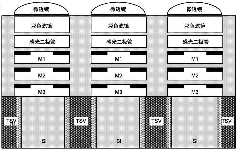
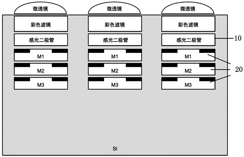
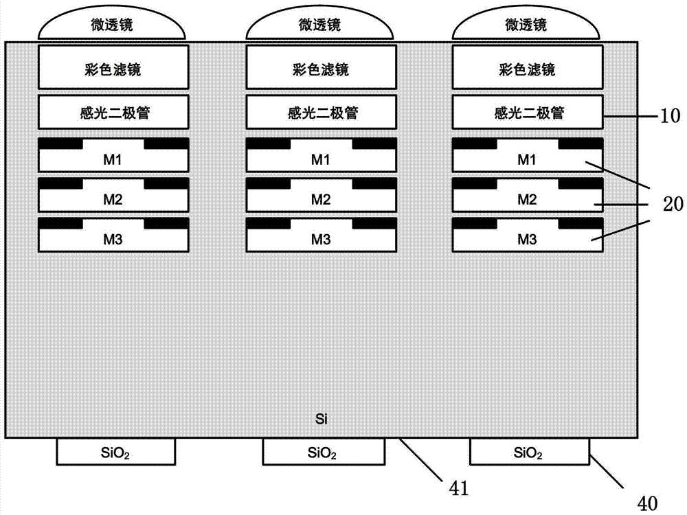
[0022] The following will refer to Figure 2 to Figure 6 A method for manufacturing a back-illuminated CMOS image sensor according to the present invention is described.

[0023] Please refer to figure 2 , firstly, a silicon substrate is provided, and a photosensitive diode region 10 for light sensing and one or more layers of metal interconnection layers 20 are sequentially formed in the substrate using a conventional back side illumination (BSI, Back Side Illumination) process. In this embodiment Among them, the number of metal interconnection layers 20 formed...


PUM

PropertyMeasurementUnit
thicknessaaaaaaaaaa

Abstract

The invention discloses a method for manufacturing a back-illuminated CMOS image sensor, which comprises sequentially forming a photosensitive diode region and at least one metal interconnection layer in a substrate; An opening area is formed between the metal interconnection layers, and the metal interconnection lines of the metal interconnection layer are drawn out through the opening area; a porous silicon structure is formed in the opening area, and the depth of the porous silicon structure is the depth from the lower surface of the substrate to the metal interconnection line; the dielectric layer is removed; and filling the porous silicon structure with conductive material. The invention has simple process and low cost, and the stress between the porous silicon structure and the substrate in the manufactured image sensor is very small, and zero mismatch can be realized.

Description

technical field [0001] The invention relates to the field of image sensors, in particular to a method for manufacturing a back-illuminated CMOS image sensor. Background technique [0002] An image sensor refers to a device that converts optical signals into electrical signals, and is an important part of a digital camera. According to the different components, it can be divided into two categories: CCD (Charge Coupled Device, charge-coupled device) and CMOS (Complementary Metal-Oxide Semiconductor, metal oxide semiconductor device). Compared with traditional CCD sensors, CMOS image sensors have the characteristics of low power consumption, low cost and compatibility with CMOS technology, so they are more and more widely used. A prerequisite for the wide application of CMOS sensors is their higher sensitivity, shorter exposure time and shrinking pixel size. [0003] Among them, the pixel sensitivity, one of the important performance indicators of CMOS image sensors, is main...

Claims


Application Information

Patent Timeline
Patent Type & Authority Patents(China)
IPC IPC(8): H01L27/146
Inventor 李琛康晓旭顾学强
Owner SHANGHAI INTEGRATED CIRCUIT RES & DEV CENT
Why Eureka
Try Eureka