Organic electroluminescence display device

A technology of electroluminescence and display devices, which is applied in the direction of circuits, electrical components, and electrical solid devices, and can solve problems such as yield reduction, pollution, and error particles.

Active Publication Date: 2013-01-23
INNOLUX CORP +1
View PDF3 Cites 9 Cited by
  • Summary
  • Abstract
  • Description
  • Claims
  • Application Information

AI Technical Summary

Problems solved by technology

This circuit is designed side by side with the light-emitting unit 110. If the aperture ratio is to be increased, the distance between the lines must be reduced (that is, the distance between the first power line 106 and the scanning line 104, and the distance between the second power line 108 and the data line 102 must be reduced

Method used


Image

  • Organic electroluminescence display device
  • Organic electroluminescence display device
  • Organic electroluminescence display device

Examples


Embodiment Construction

[0028] Implementations of the disclosed embodiments are discussed in detail below. It will be appreciated, however, that the embodiments provide many applicable inventive concepts, which can be implemented in wider variation. The specific embodiments discussed are merely intended to reveal specific ways to use the embodiments and do not limit the scope of the disclosure.

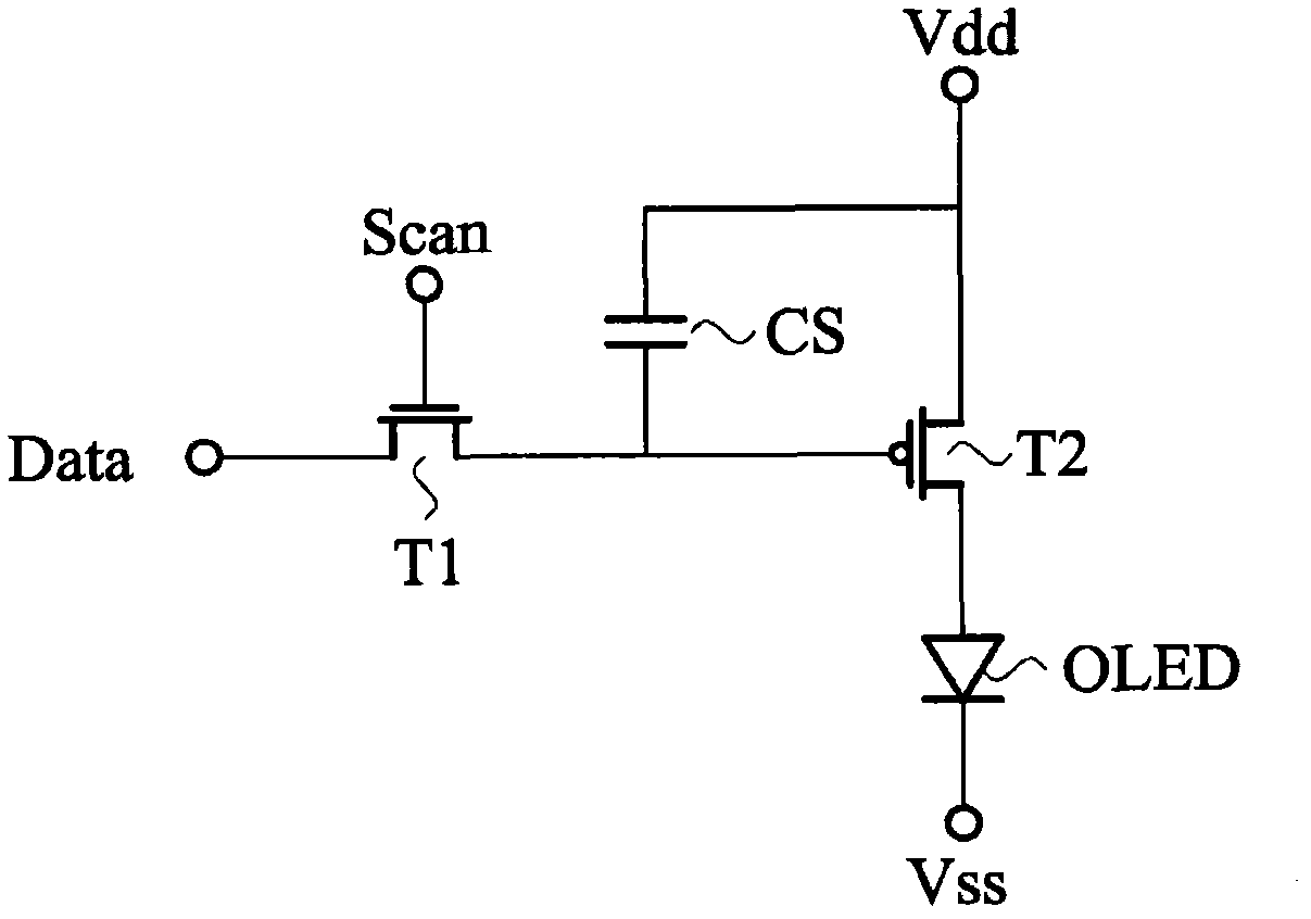
[0029] The present invention provides an organic electroluminescent display, in which signal lines (including scanning lines and data lines) and power lines are arranged on different layers, which can greatly reduce the risk of short circuits in the same layer and avoid the loss of yield rate caused thereby.

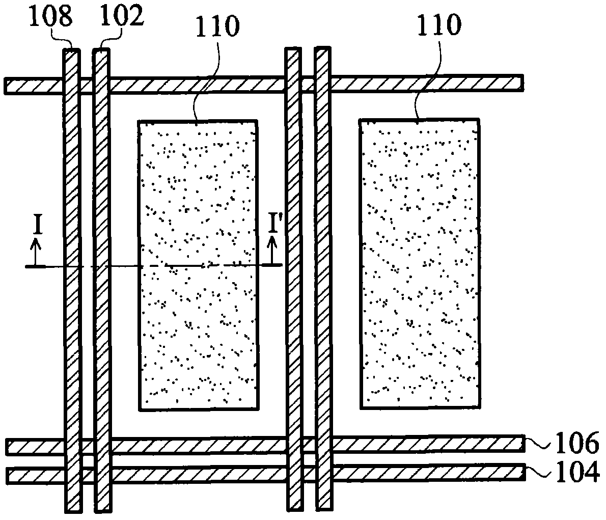
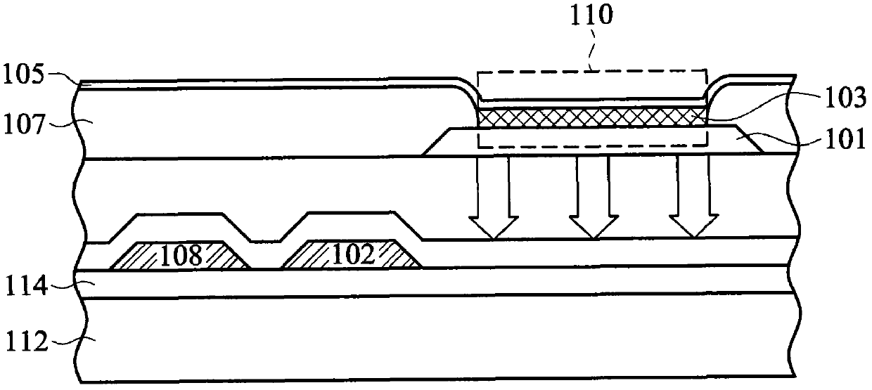
[0030] Figure 2A A plan view showing an organic electroluminescence display according to an embodiment of the present invention, Figure 2B show Figure 2A Sectional view along I-I, section line, Figure 2C Showing the plan view of the circuit configuration of the organic electroluminescence displ...


PUM


Abstract

The invention provides an organic electroluminescence display device which comprises a substrate, a plurality of interlaced power lines, a plurality of interlaced signal lines and a plurality of light emitting units, wherein the power lines and the signal lines are located on the substrate; the light emitting units are correspondingly surrounded by the power lines and the signal lines; and the power lines and the signal lines are arranged at different layers. The power lines and the signal lines are arranged at different layers, so that a certain distance is kept between the power lines and the signal lines when the aperture opening ratio is increased, then line short is not easy to occur and the yield loss is avoided.

Description

technical field [0001] The present invention relates to a display device, in particular to an organic electroluminescent display device. Background technique [0002] In recent years, organic light emission display (OLED) has been widely used in display elements of various products. The time is fast, and there is no general liquid crystal display (LCD) afterimage phenomenon and other advantages. [0003] Figure 1A It shows the circuit structure of a traditional organic electroluminescent display, in which the scan line Scan and the data line Data are electrically connected to the gate and source of the N-type thin film transistor T1, respectively, and the drain of the N-type thin film transistor T1 is electrically connected to the P-type thin film The gate of the transistor T2 is connected to one electrode of a storage capacitor CS, and the other electrode of the storage capacitor CS is electrically connected to the DC high voltage potential power line Vdd and the drain of...

Claims


Application Information

Patent Timeline
IPC IPC(8): H01L27/32
Inventor 赵光品陈韵升黄浩榕
Owner INNOLUX CORP
Why Eureka
Try Eureka