Plasma display panel

A plasma and display panel technology, applied in the direction of AC plasma display panels, discharge tubes, electrical components, etc.

Inactive Publication Date: 2013-01-23
PANASONIC CORP
View PDF1 Cites 0 Cited by
  • Summary
  • Abstract
  • Description
  • Claims
  • Application Information

AI Technical Summary

Problems solved by technology

The increase in operating voltage is an obstacle to low power drive

Method used


Image

  • Plasma display panel
  • Plasma display panel
  • Plasma display panel

Examples


Embodiment approach 1

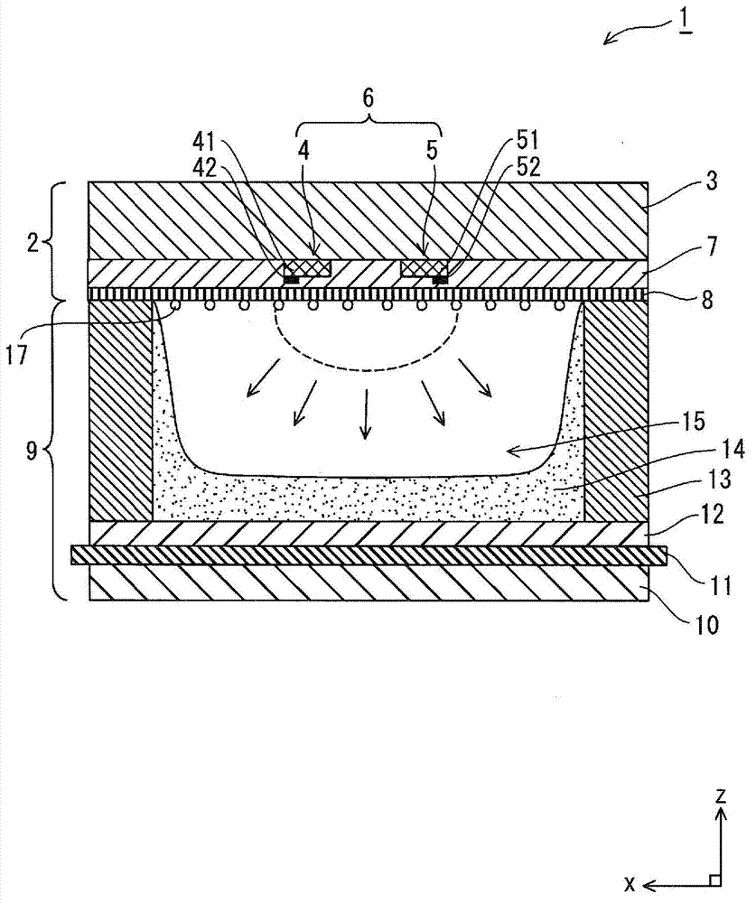
[0056] (overall structure of PDP1)

[0057] figure 1 is a schematic cross-sectional view along the xz plane of PDP1 according to Embodiment 1 of the present invention. Except for the structure around the protective film 8, the PDP1 is generally the same as the existing structure ( Figure 15 )same.

[0058] Here, the PDP 1 adopts the AC type of the NTSC standard example of the 42-inch class, but the present invention can of course be applied to other standard examples such as XGA and SXGA. As a high-definition PDP having a resolution of HD (High Definition, high definition) or higher, for example, the following specifications can be exhibited. When the panel sizes are 37, 42, and 50 inches, they can be set to 1024×720 (number of pixels), 1024×768 (number of pixels), and 1366×768 (number of pixels) in the same order. In addition, a higher resolution panel than the HD panel may also be included. As a panel having a resolution of HD or higher, a full high-definition panel eq...

Embodiment approach 2

[0104] Regarding Embodiment 2 of the present invention, differences from Embodiment 1 will be mainly described. Figure 8 It is a partially enlarged view showing the structure of the PDP 1a according to Embodiment 2 (a structure view near the front panel during driving).

[0105] The basic structure of PDP1a is the same as that of PDP1, but it is characterized in that MgO fine particles 16 with high initial electron emission characteristics are dispersedly arranged on the surface of discharge space 15 facing protective film 8 together with high γ fine particles 17 . The dispersion density of high γ fine particles 17 and MgO fine particles 16 is set so that protective film 8 is not directly seen when protective film in discharge cell 20 is viewed from the Z direction, but is not limited thereto. For example, it may be provided partially or only at the positions corresponding to the display electrode pairs 6 .

[0106] In addition, the mixing ratio of the high γ fine particles ...


PUM


Abstract

Disclosed is a PDP wherein the configuration of the periphery of a protection film is improved, excellent secondary electron emission characteristics are exhibited, and high efficiency and long service-life can be expected. Furthermore, generation of a discharge delay is eliminated when the PDP is being driven, and high-quality image display performance can be expected even in the high-speed driven and highly fine PDP. Specifically, on the dielectric layer (7) surface on the discharge space side, a crystalline film is formed as a protection film (8) to be a surface layer having a film thickness of approximately 1 [mu]m, said crystalline film having Sr at a concentration of 11.8-49.4 mol% added to CeO2. On the crystalline film, high-[gamma] fine particles (17) having secondary electron emission characteristics higher than those of the protection film is disposed, thereby improving the secondary electron emission characteristics, luminance, efficiency and reliability of the protection film.

Description

technical field [0001] The present invention relates to a plasma display panel utilizing radiation of gas discharge, and more particularly to a technique for improving the characteristics of the periphery of a surface layer (protective film). Background technique [0002] A plasma display panel (hereinafter referred to as “PDP”) is a flat-panel display device that utilizes emission from gas discharge. High-speed display and upsizing are easy, and they are widely used in fields such as video display devices and information display devices. There are direct current type (DC type) and alternating current type (AC type) in the PDP, however, the surface discharge type AC type PDP has high technical potential in terms of life characteristics and large size, and has been commercialized. [0003] Figure 15 is a schematic group diagram showing the structure of a general AC-type PDP1x. Figure 15 The shown PDP 1x is formed by bonding the front panel 2 and the rear panel 9 together. ...

Claims


Application Information

Patent Timeline
Patent Type & Authority Applications(China)
IPC IPC(8): H01J11/12H01J11/40
CPCH01J11/40H01J11/12
Inventor 福井裕介西谷干彦坂井全弘冈藤美智子奥井弥生本多洋介山内康弘井上修浅野洋
Owner PANASONIC CORP
Why Eureka
Try Eureka