Pixel driving circuit

A pixel drive circuit and capacitor technology, applied in the field of pixel circuits, can solve the problems of different brightness, the effect of screen consistency, pixel brightness inconsistency, etc., to achieve consistency improvement, improve aesthetics and competitiveness, and uniform screen brightness. Effect

Active Publication Date: 2013-01-30
CHENGDU VISTAR OPTEOLECTRONICS CO LTD
View PDF3 Cites 4 Cited by
  • Summary
  • Abstract
  • Description
  • Claims
  • Application Information

AI Technical Summary

Problems solved by technology

[0006] In the LTPS (Low Temperature Poly Silicon) process, a laser crystallization step is required. Due to the limited width of the laser, it is impossible to scan the TFTs of all pixels at one time. Therefore, it is necessary to go through multiple laser crystallization steps. The TFTs of all pixels are scanned once, but the intensity of the laser light cannot be exactly the same each time, so when the laser scans different positions, the rece

Method used


Image

  • Pixel driving circuit
  • Pixel driving circuit
  • Pixel driving circuit

Examples


Embodiment Construction

[0020] In order to facilitate a further understanding of the structure and achieved effects of the present invention, preferred embodiments are described in detail below in conjunction with the accompanying drawings.

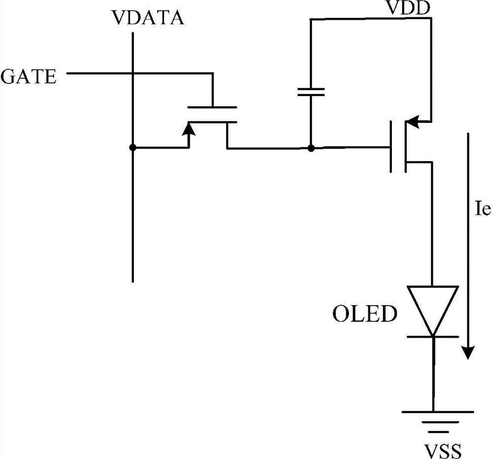
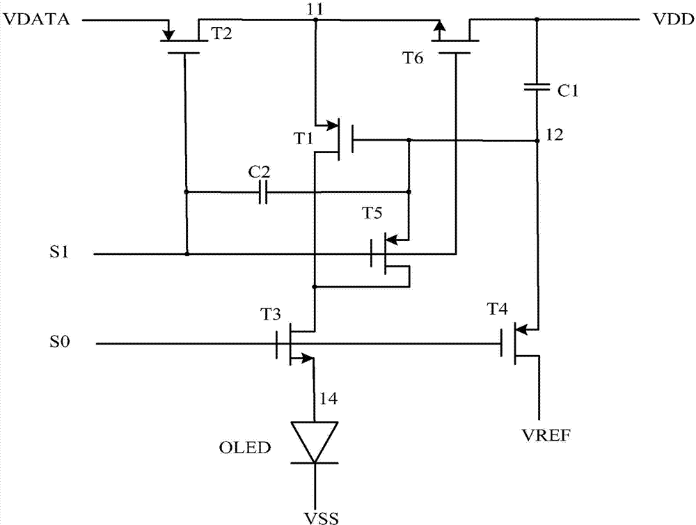
[0021] 3 is a schematic diagram of a pixel driving circuit of an active matrix organic light emitting display according to the present invention. The pixel driving circuit includes a first scanning line S0, a second scanning line S1 and a data line VDATA. The first scanning line S0 is connected to To the gate of an N-channel TFT transistor T3 and the gate of a P-channel TFT transistor T4, the second scanning line S1 is connected to the gate of a P-channel TFT transistor T5 and the gate of a P-channel TFT transistor T2 pole, the gate of an N-channel TFT transistor T6 and one end of a capacitor C2; the data line VDATA is connected to the source of the TFT transistor T2; the source of the TFT transistor T4 is connected to a reference voltage line VREF, and the TFT t...


PUM


Abstract

The invention discloses a pixel driving circuit which comprises a scanning line S0, a scanning line S1 and a data line. The S0 is connected to a grid of a thin film transistor (TFT) T3 and a grid of a TFT T4, and the S1 is connected to a grid of a TFT T5, a grid of a TFT T2, a grid of a TFT T6 and one end of a capacitor C2. The data line is connected to a source electrode of the T2, a source electrode of the T4 is connected to a reference voltage wire, a drain electrode of the T6 is connected with a voltage drain drain (VDD) wire, the VDD wire is connected with one end of a capacitor C1, and the other end of the C1 is connected to a grid of a TFT T1, the other end of the C2, a source electrode of T5 and a drain electrode of the T4. A source electrode of the T1 is connected to a drain electrode of the T2 and a source electrode of the T6, a drain electrode of the T3 is connected to a drain electrode of the T1 and a drain electrode of the T5, A source electrode of the T3 is connected to an anode of an organic light-emitting diode (OLED), and a cathode of the OLED is connected to a negative voltage VSS. The pixel driving circuit enables brightness of a screen body to be uniform and consistent, and a narrow frame of the screen body can be achieved.

Description

technical field [0001] The present invention relates to a pixel circuit, in particular to an AMOLED pixel drive circuit capable of making the brightness of Active Matrix Organic Light Emitting Diode (AMOLED, Active Matrix Organic Light Emitting Diode) more uniform. Background technique [0002] Organic light-emitting diode (OLED) is an active light-emitting device. Compared with the current mainstream flat-panel display technology thin-film field-effect transistor liquid crystal display (TFT-LCD), OLED has the advantages of high contrast, wide viewing angle, low power consumption and thinner volume. It becomes the next-generation flat-panel display technology after LCD, and is one of the most concerned technologies in flat-panel display technology. [0003] For an active organic light-emitting display (AMOLED), FIG. 1 is a schematic diagram of a pixel circuit in the prior art, and FIG. 2 is a working timing diagram of a pixel circuit in the prior art. The brightness of the ...

Claims


Application Information

Patent Timeline
IPC IPC(8): G09G3/32G09G3/3233
Inventor 胡思明邱勇黄秀颀高孝裕永井肇
Owner CHENGDU VISTAR OPTEOLECTRONICS CO LTD
Why Eureka
Try Eureka