AlN substrate-based graphene CVD direct epitaxial growth method and manufactured device
A technology of epitaxial growth and graphene, which is applied in semiconductor/solid-state device manufacturing, electrical components, circuits, etc., can solve the problems that affect the electrical characteristics of graphene devices, it is difficult to transfer graphene cleanly, reduce the mobility of graphene, etc., to achieve Effects of improving reliability and electrical characteristics, simplifying growth steps and device manufacturing process steps, and reducing manufacturing costs
- Summary
- Abstract
- Description
- Claims
- Application Information
AI Technical Summary
Problems solved by technology
Method used
Image

Examples
Embodiment 1
[0022] The realization steps of the present invention are as follows:
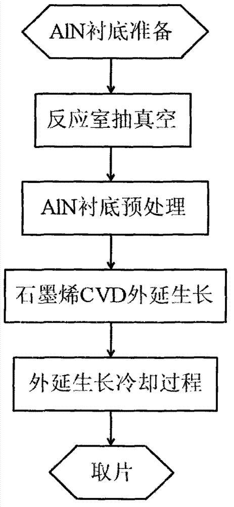
[0023] Step 1, AlN substrate preparation.
[0024] Put the AlN substrate into acetone, ethanol and deionized water successively for cleaning, each time for 10 minutes, take out the substrate from the deionized water, and dry it with high-purity nitrogen (99.9999%).
[0025] Step 2, vacuumize the reaction chamber.
[0026] Place the AlN substrate of semiconductor device level in the chemical vapor deposition CVD reaction chamber, and pump the vacuum to 10 -6 Torr to remove residual gas in the reaction chamber.
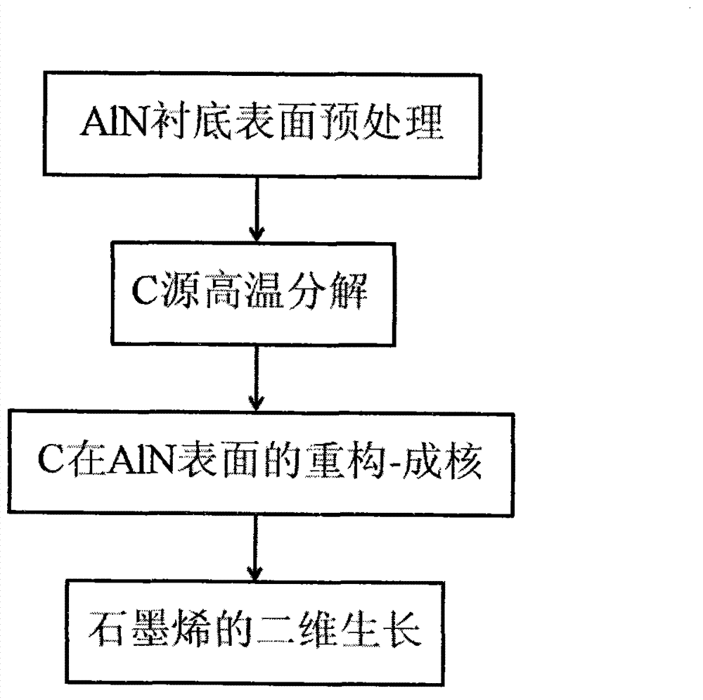
[0027] Step 3, AlN substrate surface pretreatment.
[0028] Introduce H into the reaction chamber 2 The substrate surface pretreatment was carried out, the gas flow rate was 2 sccm, the vacuum degree of the reaction chamber was 0.1 Torr, the substrate temperature was 950° C., and the processing time was 5 minutes.
[0029] Step 4, graphene CVD epitaxial growth.
[0030] Introduce Ar and CH int...
Embodiment 2
[0034] The realization steps of the present invention are as follows:
[0035] Step A, A1N substrate preparation.
[0036] The AlN substrate was washed in acetone, ethanol and deionized water successively, each time for 20 minutes, the substrate was taken out from the deionized water, and dried with high-purity nitrogen (99.9999%).
[0037] In step B, the reaction chamber is evacuated.
[0038] Place the AlN substrate of semiconductor device level in the chemical vapor deposition CVD reaction chamber, and pump the vacuum to 10 -6 Torr to remove residual gas in the reaction chamber.
[0039] Step C, pretreating the surface of the AlN substrate.
[0040] Introduce H into the reaction chamber 2 The substrate surface pretreatment was carried out, the gas flow rate was 5 sccm, the vacuum degree of the reaction chamber was 0.2 Torr, the substrate temperature was 950° C., and the processing time was 10 minutes.
[0041] Step D, graphene CVD epitaxial growth.
[0042] Introduce ...
Embodiment 3
[0046] The realization steps of the present invention are as follows:
[0047] Step 1, the AlN substrate is prepared.
[0048]The AlN substrate was washed in acetone, ethanol and deionized water successively, each time for 30 minutes, the substrate was taken out from the deionized water, and dried with high-purity nitrogen (99.9999%).
[0049] Step 2, the reaction chamber is evacuated.
[0050] Place the AlN substrate of semiconductor device level in the chemical vapor deposition CVD reaction chamber, and pump the vacuum to 10 -6 Torr to remove residual gas in the reaction chamber.
[0051] Step 3, pretreatment of the surface of the AlN substrate.
[0052] Introduce H into the reaction chamber 2 The substrate surface pretreatment was carried out, the gas flow rate was 5 sccm, the vacuum degree of the reaction chamber was 0.2 Torr, the substrate temperature was 1000° C., and the processing time was 8 minutes.
[0053] Step 4, graphene CVD epitaxial growth.
[0054] Introd...
PUM
 Abstract
Description
Claims
Application Information
 - R&D Engineer
- R&D Manager
- IP Professional
- Industry Leading Data Capabilities
- Powerful AI technology
- Patent DNA Extraction
Browse by: Latest US Patents, China's latest patents, Technical Efficacy Thesaurus, Application Domain, Technology Topic.
© 2024 PatSnap. All rights reserved.Legal|Privacy policy|Modern Slavery Act Transparency Statement|Sitemap