Transparent conducting electrode based on graphene and manufacture method and applications thereof

A technology of transparent conductive electrodes and graphene, applied in circuits, electrical components, semiconductor devices, etc., can solve problems such as optical performance degradation, ion diffusion, device damage, etc., and achieve low cost and expand application effects

Inactive Publication Date: 2010-10-13
SUZHOU INST OF NANO TECH & NANO BIONICS CHINESE ACEDEMY OF SCI
View PDF3 Cites 110 Cited by
  • Summary
  • Abstract
  • Description
  • Claims
  • Application Information

AI Technical Summary

Problems solved by technology

However, the use of ITO is facing more and more serious problems
Since In in ITO is expected to be exhausted on the earth within 10 years, the price of In has been as high as $1,000 / kg in recent years, and the demand for ITO from electronics manufacturers has increased, making the price of ITO very expensive
In addition to becoming rarer and more expensive, ITO is prone to ion diffusion in the presence of acids and alkalis. Its use is harmful to the manufacturing plant environment and human health. At the same time, ions diffuse into the polymer insulating layer of the device, resulting in optical performance. drop, or even leakage leads to device damage

Method used


Image

  • Transparent conducting electrode based on graphene and manufacture method and applications thereof
  • Transparent conducting electrode based on graphene and manufacture method and applications thereof
  • Transparent conducting electrode based on graphene and manufacture method and applications thereof

Examples


Embodiment 1

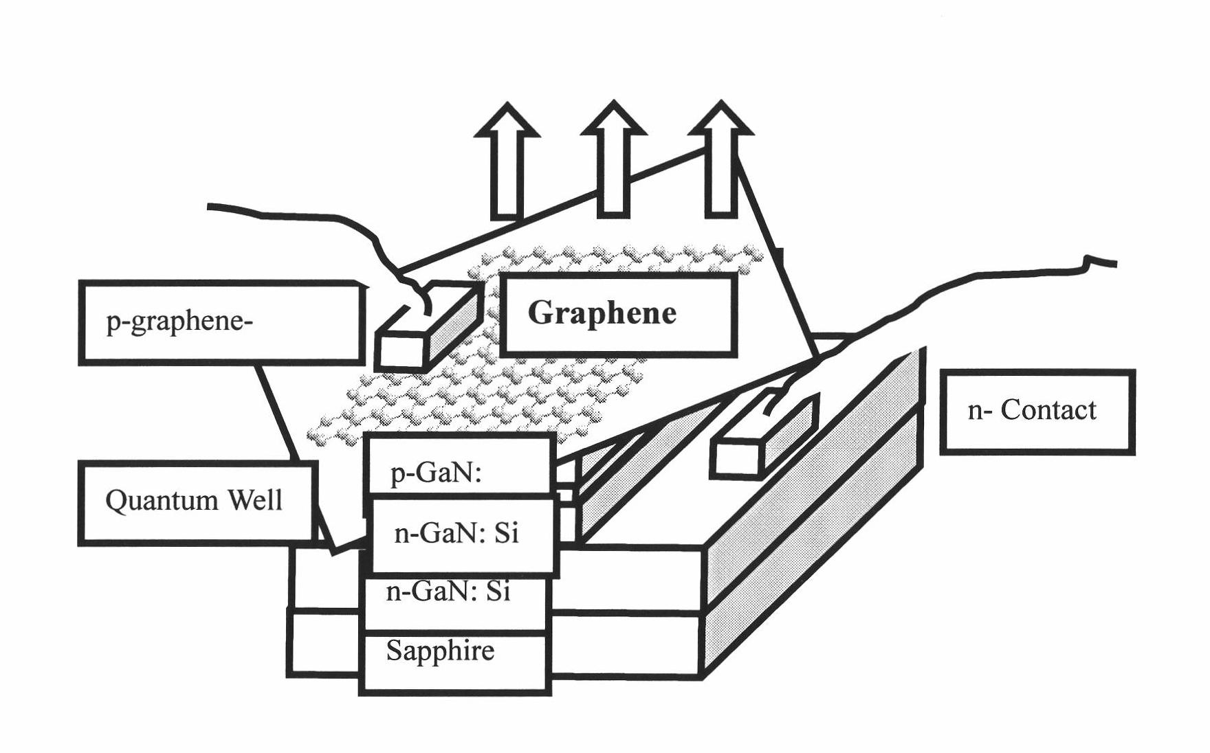
[0038] See attached description figure 1 , Graphene thin films make transparent conductive electrodes for GaN-based LEDs.

[0039] (1) on Si / SiO 2 Electron beam evaporation, magnetron sputtering or thermal evaporation of 100nm-500nm metal Ni film on the substrate is used as a catalyst for chemical vapor deposition and placed in a tube furnace. After reduction for 20 minutes, methane was introduced, the reaction time was 3-5 minutes, methane was stopped, the temperature was lowered under the protection of hydrogen, and the sample was taken out.

[0040] (2) Place the grown GaN epitaxial wafer containing quantum wells in a tube furnace, N 2 Keep at 750° C. for 15 minutes under ambient conditions to activate the Mg-doped P-type GaN layer.

[0041] (3) Place BOE(H 2 SO 4 :H 2 o 2 =3:1) in the solution at 70°C for 3 minutes, and keep at 120°C on the hot plate for 5 minutes to remove the residual solution.

[0042] (4) Take Si / SiO 2 After growing the graphene sample on the ...

Embodiment 2

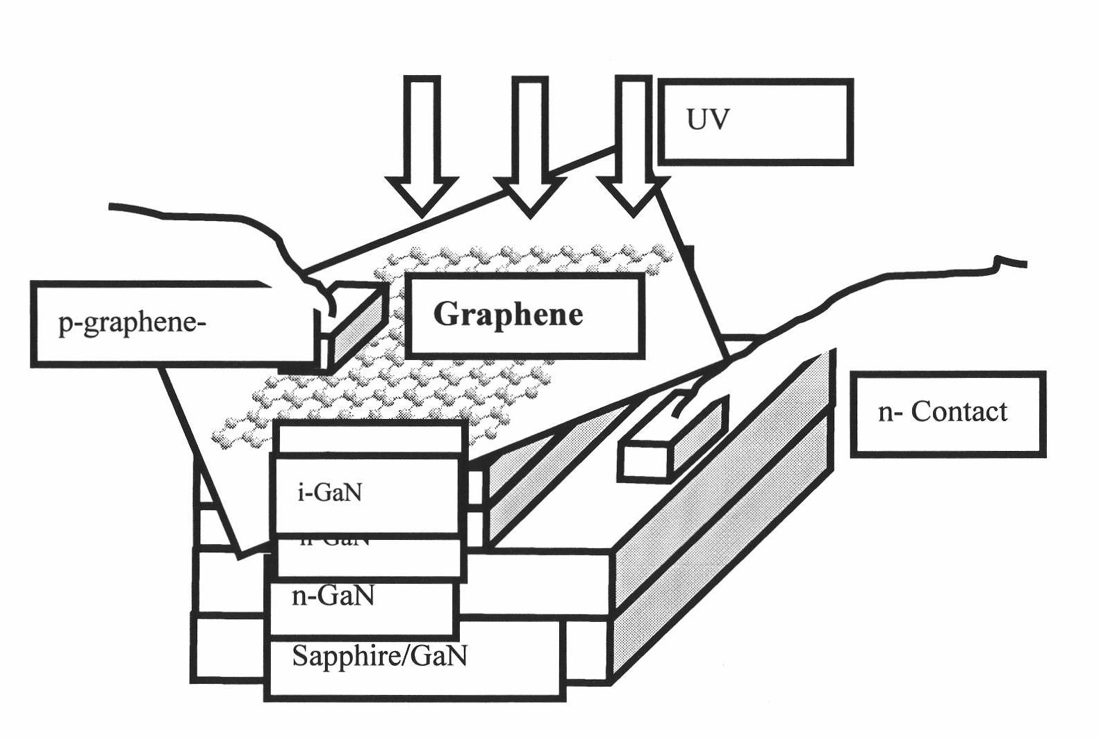
[0059] See attached description figure 2 , Graphene thin films make transparent conductive electrodes for GaN-based ultraviolet photodetectors.

[0060] (1) on Si / SiO 2 Electron beam evaporation, magnetron sputtering or thermal evaporation of 100nm-500nm metal Ni film on the substrate is used as a catalyst for chemical vapor deposition and placed in a tube furnace. After reduction for 20 minutes, methane was introduced, the reaction time was 3-5 minutes, methane was stopped, the temperature was lowered under the protection of hydrogen, and the sample was taken out.

[0061] (2) Place the p-i-n GaN epitaxial wafer in the tube furnace, N 2 Keep at 750° C. for 15 minutes under ambient conditions to activate the Mg-doped P-type GaN layer.

[0062] (3) Place BOE(H 2 SO 4 :H 2 o 2 =3:1) in the solution at 70°C for 3 minutes, and keep at 120°C on the hot plate for 5 minutes to remove the residual solution.

[0063] (4) Take Si / SiO 2 After growing the graphene sample on the ...


PUM

PropertyMeasurementUnit
sizeaaaaaaaaaa
sizeaaaaaaaaaa
electrical conductivityaaaaaaaaaa

Abstract

The invention discloses a transparent conducting electrode using a graphene film as a GaN-based LED (light-emitting diode) or ultraviolet light detector and a manufacture method and applications thereof. The graphene film is solidified and bonded on the surface of the GaN substrate of the LED or ultraviolet light detector. The transparent graphene conducting film is prepared by adopting a chemical vapor deposition or reduction-oxidation method, and the GaN-based LED or ultraviolet light detector is manufactured by utilizing a micromachining photoetching, etching and metal deposition method; the graphene film is moved to the p-type GaN-based substrate of the LED or ultraviolet light detector to serve as the transparent conducting electrode instead of ITO or Ni/Au. In the invention, the graphene film is used as the transparent conducting electrode, which can realize low-cost and high-brightness luminescent devices and expands the applications of carbon nanometer materials in the field of GaN-based photoelectric devices.

Description

technical field [0001] The invention relates to a GaN-based LED, a transparent conductive electrode of an ultraviolet light detector and a manufacturing method thereof. The manufacturing process includes preparing a graphene film, transferring the graphene film to a P-type GaN substrate, and micromachining the detector. A transparent conductive electrode belongs to the technical field of carbon nanotubes. Background technique [0002] In 2004, the A.K.Geim group of the University of Manchester in the United Kingdom made a breakthrough in the preparation of graphite samples with a single atomic layer thickness by mechanical exfoliation. They report the phenomenon of field-effect electron transport in monolayer graphite [3] . Subsequently, in 2005, the Geim group and the P.Kim group of Columbia University in the United States successively reported that the integer quantum Hall effect was observed in single-layer graphite samples. In particular, the integer quantum Hall effe...

Claims


Application Information

Patent Timeline
Patent Type & Authority Applications(China)
IPC IPC(8): H01L33/42H01L31/0224H01L31/18
CPCY02P70/50
Inventor 刘立伟邢振远牛亮宋仁升荣吉赞赵勇杰耿秀梅李伟伟程国胜
Owner SUZHOU INST OF NANO TECH & NANO BIONICS CHINESE ACEDEMY OF SCI
Why Eureka
Try Eureka