PCB (printed circuit board) structure available for grafting and transplanting and PCB structure grafting method

A PCB board and motherboard technology, which is applied to the graftable and transplantable PCB board structure and the field of grafting, can solve the problems of weak connection of the circuit board, poor appearance quality, increased production cost, etc., and achieves great economy and environmental protection. Simple structure and the effect of improving production efficiency

Inactive Publication Date: 2013-01-30
深圳市亿铖希科技有限公司
View PDF2 Cites 8 Cited by
  • Summary
  • Abstract
  • Description
  • Claims
  • Application Information

AI Technical Summary

Problems solved by technology

[0002] At present, due to various reasons in the production process of multi-piece PCB boards, it is inevitable that a single or several units have defects, resulting in unit scrapping; component placement is a multi-piece operation, and the scrapped units are also mounted with electronic components during the operation. devices, resulting in unnecessary waste of resources
However, to solve this problem in the industry, in-line bonding technology is often used to repair and replace unqualified sub-circuit boards, but this existing technology will lead to poor connection of circuit boards, low alignment accuracy, poor appearance quality, complicated procedures, and excessive costs. High-level problems, and in order to achieve the purpose of firmly bonding the PCB board, many manufacturers use high-quality adhesives to bond the joint parts to make up for the defects in the mechanical connection of the joint parts, which increases the production cost of the enterprise

Method used


Image

  • PCB (printed circuit board) structure available for grafting and transplanting and PCB structure grafting method
  • PCB (printed circuit board) structure available for grafting and transplanting and PCB structure grafting method
  • PCB (printed circuit board) structure available for grafting and transplanting and PCB structure grafting method

Examples


Embodiment Construction

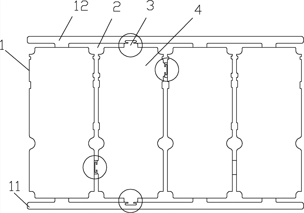
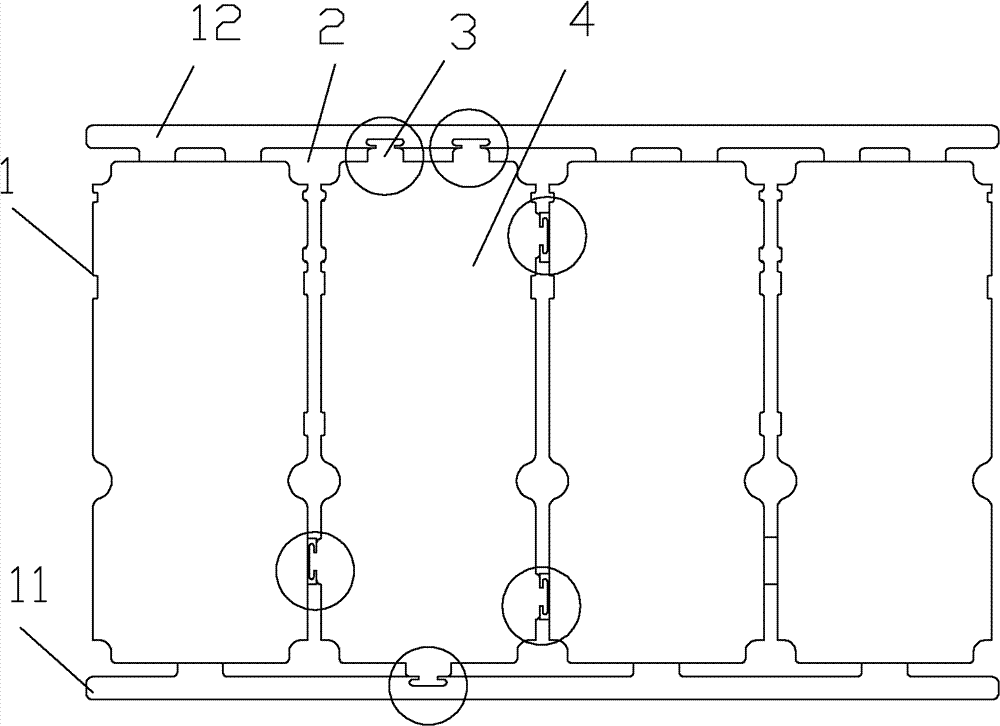
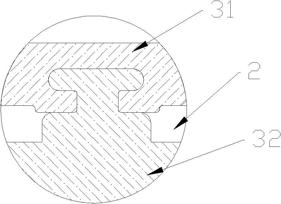
[0025] Such as figure 1 As shown, the embodiment of the present invention provides a graftable PCB board structure, including a grafting mother board 1 and a grafting daughter board 4, the grafting mother board 1 is a multi-piece PCB board to be grafted, and the grafting daughter board 4 is a qualified PCB board unit. The grafting mother board 1 is provided with a working side A11 and a working side B12. The working side is respectively provided with a concave groove 31, and the grafting sub-board 4 is provided with a working side Corresponding two convex interfaces 32; the grafted sub-board 4 overlaps with the concave slot 31 on the grafted motherboard 1 through the convex interface 32; on the grafted motherboard 1, two adjacent units of the PCB board unit to be grafted A concave slot 31 is provided respectively, and two convex interfaces 32 matched with the concave slot 31 of the PCB unit to be grafted are also provided on the graft sub-board 4 , and the graft sub-board 4 pa...


PUM


Abstract

The invention discloses a PCB (printed circuit board) structure available for grafting and transplanting. The PCB structure comprises a master grafting board and a slave grafting board, the master grafting board is provided with an operating side which is provided with at least one concave clamping groove, the slave grafting board is provided with at least one convex connector, and the slave grafting board is coincided with the concave clamping grooves through the convex connectors. The invention further discloses a grafting method for the PCB structure available for grafting and transplanting. The method includes the technical procedures: removing defective units; selecting the slave grafting board; planting the selected slave grafting board at the defective unit position of the master grafting board, and leveling the slave grafting board and the master grafting board on the same plane; and adding macromolecule adhesives at the joint. Accepted products of multi-layer PCBs which meet the requirements can be processed by the grafting method for the PCB structure available for grafting and transplanting, the precision and reliability requirements can be met, the integral appearances of the multi-layer PCBs are unaffected, production efficiency is improved, production cost is reduced, and great economy and environment friendliness are achieved.

Description

technical field [0001] The invention relates to a grafting structure and a grafting method of defective units of multiple PCB boards, in particular to a graftable and transplantable PCB board structure and a grafting method thereof. Background technique [0002] At present, due to various reasons in the production process of multi-piece PCB boards, it is inevitable that a single or several units have defects, resulting in unit scrapping; component placement is a multi-piece operation, and the scrapped units are also mounted with electronic components during the operation. devices, resulting in unnecessary waste of resources. However, to solve this problem in the industry, in-line bonding technology is often used to repair and replace unqualified sub-circuit boards, but this existing technology will lead to poor connection of circuit boards, low alignment accuracy, poor appearance quality, complicated procedures, and excessive costs. High-level problems, and in order to achi...

Claims


Application Information

Patent Timeline
Patent Type & Authority Applications(China)
IPC IPC(8): H05K1/14H05K3/36
Inventor 文丹
Owner 深圳市亿铖希科技有限公司
Why Eureka
Try Eureka