Array substrate and driving method of pixels

A technology of an array substrate and a driving method, which is applied in the field of liquid crystal display, can solve problems such as screen display problems and delays, and achieve voltage stability and avoid jump voltage effects

Active Publication Date: 2013-02-13
BOE TECH GRP CO LTD
View PDF7 Cites 19 Cited by
  • Summary
  • Abstract
  • Description
  • Claims
  • Application Information

AI Technical Summary

Problems solved by technology

In the pixel area of ​​TFS mode, a pixel area is formed by the intersection of a gate line (Gate) and two data lines (Data), that is, a 1G2D structure; usually, the data line of the pixel area is connected to the source, and the data line The voltage is applied to the line by the driving circuit, and the signal is transmitted to the pixel electrode through the TFT switch; however, in the array substrate in the new TFS mode, the two data lines will respectively generate coupling capacitance with the pixel electrode, and for two data lines with the same voltage As far as the line is concerned, the coupling capacitance between the data line and the pixel electrode is the sum of the coupling capacitances between the two data lines and the pixel electrode respectively. Due to the existence of the coupling capacitance, the signal transmitted from the data line to the pixel electrode has A certain delay, resulting in problems with the screen display

Method used


Image

  • Array substrate and driving method of pixels
  • Array substrate and driving method of pixels
  • Array substrate and driving method of pixels

Examples


Embodiment Construction

[0039] In order to better illustrate the technical problem to be solved by the present invention, the working principle provided by the present invention is first described in detail.

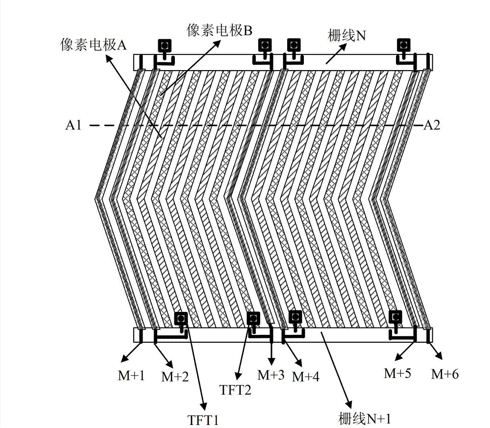
[0040] Such as figure 1 As shown, it is a plan view of the pixel area of ​​the TFS mode array substrate according to the embodiment of the present invention. The array substrate provided by the embodiment of the present invention includes: gate lines and data lines, and one gate line and two data lines define the pixel area ( That is, the structure of 1G2D), the gate line and the data line can be vertically intersected to form a limited pixel area, or the data line can also be a zigzag type that crosses the gate line to define the pixel area, and two thin films are formed at the intersection of the gate line and the data line Transistors (that is, two TFTs), with pixel electrodes arranged at intervals in the pixel area, wherein the first thin film transistor (such as figure 1 TFT1 shown in ) i...


PUM

PropertyMeasurementUnit
widthaaaaaaaaaa

Abstract

The invention provides an array substrate and a driving method of pixels. The array substrate comprises a grid line and data lines, the grid line and two data lines define a pixel area, two thin film transistors are formed at a crossing position, and pixel electrodes arranged at intervals are arranged in the pixel area. A first thin film transistor in the two thin film transistors is connected with a first pixel electrode, and a second thin film transistor is connected with a second pixel electrode. The array substrate is characterized in that equal voltage with opposite polarities are exerted onto the first pixel electrode and the second pixel electrode respectively through the first thin film transistor and the second thin film transistor. An embodiment of the array substrate and the driving method of pixels can avoid a phenomenon that image display is uneven due to leaping voltage caused by coupling capacitance between the data lines and the pixel electrodes.

Description

technical field [0001] The invention relates to the field of liquid crystal display, in particular to an array substrate and a driving method for pixels. Background technique [0002] In the field of display technology, Advanced Super Dimension Switch technology (ADvanced Super Dimension Switch) can improve the picture quality of TFT-LCD products, with high resolution, high transmittance, low power consumption, wide viewing angle, high aperture ratio, and low color difference , No extrusion water ripple (push Mura) and other advantages. Therefore, it is widely used in various display products. Advanced ultra-dimensional field conversion technology is the core technology of planar electric field wide viewing angle, that is, the electric field generated by the edge of the slit electrode in the same plane and the generation between the slit electrode layer and the plate electrode layer The electric field in the liquid crystal cell forms a multi-dimensional electric field, so t...

Claims


Application Information

Patent Timeline
Patent Type & Authority Applications(China)
IPC IPC(8): G02F1/1362G02F1/1368G02F1/133G09G3/36
CPCG09G3/3614G02F1/133G09G2300/0426G09G2320/0233
Inventor 严允晟崔贤植徐智强李会
Owner BOE TECH GRP CO LTD
Why Eureka
Try Eureka