Method for forming pad structure

A pad and graphic transfer technology, which is applied in the direction of electrical components, electrical solid devices, circuits, etc., can solve the problems of time-consuming production cost and complicated process flow, and achieve the effect of simple process, good compatibility, and time-saving production cost

Active Publication Date: 2013-02-13
SEMICON MFG INT (SHANGHAI) CORP
View PDF6 Cites 2 Cited by
  • Summary
  • Abstract
  • Description
  • Claims
  • Application Information

AI Technical Summary

Problems solved by technology

However, this patent introduces complex structures such as the formation of diffusion barrier layers, seed layers, and under-ball metal layers, and the process is complicated, so time-consuming and high production costs

Method used


Image

  • Method for forming pad structure
  • Method for forming pad structure
  • Method for forming pad structure

Examples


no. 1 example

[0061] The following combination Figure 7 The flow chart of the method for forming the pad structure shown in the flowchart describes in detail how to form the pad structure provided by the first embodiment of the present invention.

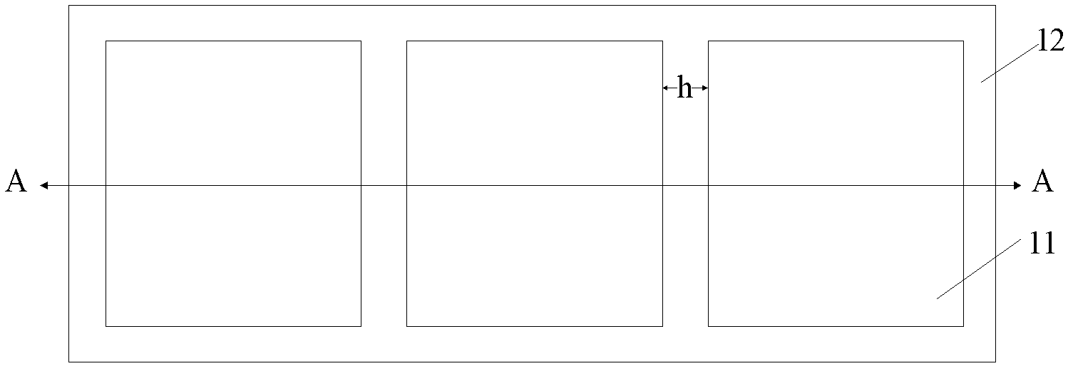
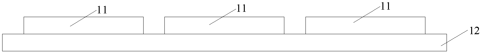
[0062] Firstly, step S21 is executed to provide a substrate 20 . Structural cross-section as Figure 8 As shown, there are three aluminum pads 21 on the substrate 20 . The substrate 20 includes a device structure, and the device structure is electrically connected to the aluminum pad 21 as required.

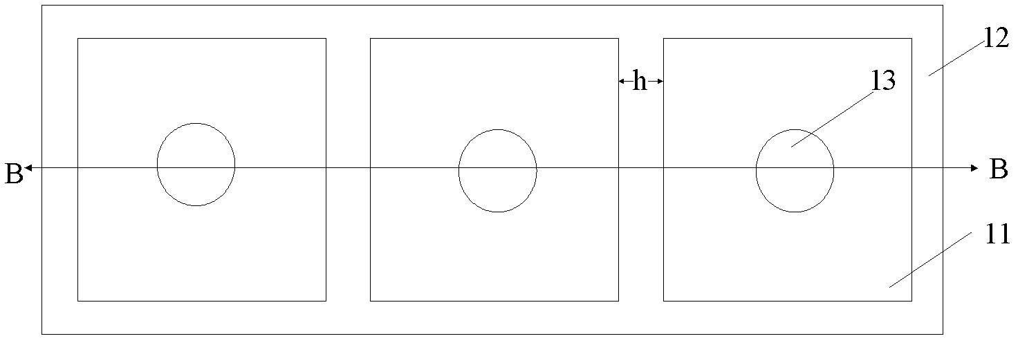
[0063] Executing step S22, forming a first protective layer 22 on the substrate 20 and the aluminum pad 21, the formed structure is as follows Figure 9 shown. The first protective layer 22 is an insulating material, which may be photoresist, such as photosensitive polyimide. Polyimide is an oily material, its hydrophobic property can isolate water vapor, and its C-N structure can absorb radiated light, so as to prevent the devices on the alum...

no. 2 example

[0085] Embodiment 2 of the present invention provides another method for forming a pad structure, the flow chart is as follows Figure 18 shown. The following pair Figure 18 The flow shown is described in detail.

[0086] Firstly, step S41 is performed to provide a substrate 20, on which there are three aluminum pads 21, the structural cross-sectional view is as follows Figure 8 shown. This step is the same as step S21 in the first embodiment.

[0087] Execute step S42, forming a protective layer 29 on the substrate 20 and the aluminum pad 21, the structural cross-sectional view is as follows Figure 9 shown. in, Figure 9 The number 22 in is the second protective layer. Since the protective layer is only formed once in the second embodiment, those skilled in the art need to understand Figure 9 The reference number 22 is replaced by 29; the formation method and material of the protective layer 29 in this step are the same as the formation method and material of the s...


PUM


Abstract

The invention provides a method for forming a pad structure. The method comprises the following steps of: providing a substrate, wherein the substrate is provided with a first protection layer and pads exposed from the first protection layer; forming a second protection layer on the first protection layer and the pads; forming first openings on the second protection layer to expose the pads, wherein the bottoms of the first openings are positioned on the pads; and filling the first openings with a solder material to form new pads. By the method for forming the pad structure, the requirement of flip chip bonding on the pads can be met, the process is simple, time is saved, and production cost is low.

Description

technical field [0001] The invention relates to the field of semiconductor manufacturing, in particular to a method for forming a pad structure. Background technique [0002] In the manufacture of integrated circuits, semiconductor chips are ultimately combined with other chips or other electronic components on printed circuit boards to perform their functions. At present, there are mainly two methods for chip bonding, one is wire bonding, and the other is flip chip bonding. Wire bonding is performed by connecting the I / O bumps on eg aluminum pads of one chip to the I / O bumps on the aluminum pads of another chip through connecting wires. Flip-chip bonding is achieved by covering the input / output bumps on the pads of one chip with solder material, typically solder bumps, then flipping the other chip over and Cover the solder balls, then put them in the reflow furnace, and solder to form the input / output combination of the upper and lower chip pads. [0003] figure 1 It is...

Claims


Application Information

Patent Timeline
Patent Type & Authority Applications(China)
IPC IPC(8): H01L23/00H01L21/60
CPCH01L2224/10H01L2224/73204
Inventor 丁海涛
Owner SEMICON MFG INT (SHANGHAI) CORP
Why Eureka
Try Eureka