Method for manufacturing longitudinal power semiconductor device

A technology of power semiconductors and manufacturing methods, applied in semiconductor/solid-state device manufacturing, semiconductor devices, electrical components, etc.

Active Publication Date: 2013-02-27
UNIV OF ELECTRONICS SCI & TECH OF CHINA
View PDF6 Cites 5 Cited by
  • Summary
  • Abstract
  • Description
  • Claims
  • Application Information

AI Technical Summary

Problems solved by technology

[0011] The purpose of the present invention is to overcome the shortcomings of the relatively difficult manufacturing process of semiconductor power devices with trench-gate superjunctions, and to provide a method for manufacturing vertical power semiconductor devices

Method used


Image

  • Method for manufacturing longitudinal power semiconductor device
  • Method for manufacturing longitudinal power semiconductor device
  • Method for manufacturing longitudinal power semiconductor device

Examples


Embodiment 1

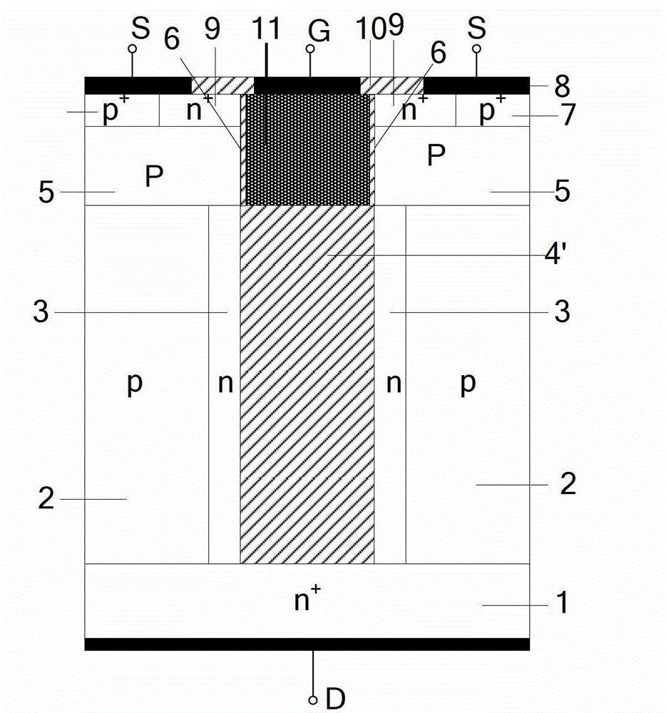
[0065] This example takes the manufacture of N-channel trench gate VDMOS with a dielectric trench as an example to describe in detail the manufacturing method of the vertical power semiconductor device of the present invention. The structural schematic diagram of the N-channel trench gate VDMOS with a dielectric trench is as follows Figure 5 .

[0066] In this example, the method for manufacturing an N-channel trench gate VDMOS with a dielectric trench includes the following specific steps:

[0067] a. By epitaxial growth, an n-type first semiconductor region 2 is formed on the N+ semiconductor substrate 1, and after the first semiconductor region 2 is formed, it is as follows Figure 6 shown;

[0068] b. Thermally oxidize and grow a thin oxide layer 13 on the top of the first semiconductor region 2, and then deposit Si 3 N 4 Masking layer 14, then coat photoresist 15 again, carry out photoetching, coat photoresist 15 after being coated with as Figure 7 shown;

[0069] ...

Embodiment 2

[0085] This example takes the manufacture of IGBT devices as an example, and its structure diagram is as follows Figure 20 shown.

[0086] The manufacturing process of the semiconductor device of the present invention described in detail in Embodiment 1 is preferably applied to MOS-controlled vertical devices, so as to alleviate the contradictory relationship among withstand voltage, on-resistance and switching loss. And applied in such as Figure 20 In the shown IGBT device, the conductivity type of the semiconductor substrate 1 is opposite to that of the second semiconductor region 3. For the n-channel IGBT, the difference from Example 1 is that the initial material of the semiconductor substrate 1 is P + The conductivity type of the semiconductor substrate 101 is opposite to that of the second semiconductor region 3 , and the rest of the steps are exactly the same as those of the first embodiment.

Embodiment 3

[0088] This example takes the manufacture of P-channel trench-gate VDMOS devices as an example, and its structure diagram is as follows Figure 21 shown.

[0089] The manufacturing process of the semiconductor device of the present invention described in detail in Embodiment 1 can be applied to control vertical devices of N-channel MOS, and can also be applied to control vertical devices of P-channel MOS. Such as Figure 21 As shown, the doping type of the semiconductor substrate 1, the second semiconductor region 3 formed by oblique ion implantation, the body region 5, the body contact region 7, the source region 9 and the corresponding region of the N-channel VDMOS described in Embodiment 1 Just the opposite.


PUM


Abstract

The invention relates to semiconductor technology, aims to overcome the difficulty of manufacturing a semiconductor power device with a trench / gate super-junction, and provides a method for manufacturing a longitudinal power semiconductor device. The technical scheme of the invention is as follows: firstly a first semiconductor region is formed by epitaxial process; a first oxide layer and a deposited mask layer are formed at the top of the first semiconductor region, the photoetching operation is performed, a first trench is formed by etching, a second oxide layer is formed on the two side walls of the first trench, the second oxide layer is removed by wet-etching, a third oxide layer is formed on the inner wall of the trench, a second semiconductor region is formed on the two side walls of the first trench, the third oxide layer is removed, a fourth oxide layer is formed, insulation dielectrics are packed and then planarization is carried out, a body region is formed, a second trench is formed on the body region by etching, a trench gate is made, and finally a source region and a body contact region are formed, followed by electrode preparation and surface passivation. The method has the benefits of having low process difficulty and being applied to MOS-controlled longitudinal devices.

Description

technical field [0001] The invention relates to semiconductor technology, in particular to a method for manufacturing a vertical power semiconductor device. Background technique [0002] Power MOSFET is a multi-subconduction device, which has many advantages such as high input impedance, high frequency, and positive temperature coefficient of on-resistance. These advantages make it widely used in the field of power electronics, greatly improving the efficiency of electronic systems. [0003] The high voltage resistance of the device requires a long drift region and a low doping concentration in the drift region. However, as the length of the drift region increases and the doping concentration decreases, the on-resistance (R on ) increases, the on-state power consumption increases, and the device on-resistance R on There is the following relationship with the breakdown voltage BV: that is, R on ∝BV 2.5 . [0004] With the advancement of the manufacturing process, the ce...

Claims


Application Information

Patent Timeline
Patent Type & Authority Applications(China)
IPC IPC(8): H01L21/28H01L21/336
Inventor 罗小蓉周坤范叶范远航蒋永恒王沛王骁玮罗尹春蔡金勇张波
Owner UNIV OF ELECTRONICS SCI & TECH OF CHINA
Why Eureka
Try Eureka