
A semiconductor module structure and a method for connecting and fixing bonding wires in the structure

A technology of module structure and bonding wire, applied in semiconductor/solid-state device manufacturing, semiconductor/solid-state device components, semiconductor devices, etc., can solve problems such as shortening the service life of modules, breakage of bonding feet, module failure, etc., and achieve the elimination cycle Vibration, prolong service life, and ensure the effect of reliability

Active Publication Date: 2015-08-19
XIAN YONGDIAN ELECTRIC
View PDF3 Cites 0 Cited by
  • Summary
  • Abstract
  • Description
  • Claims
  • Application Information

AI Technical Summary

Problems solved by technology

However, in the packaging of power semiconductor modules, the bonding aluminum wires are limited by the flow capacity, and often multiple bonding aluminum wires are gathered together with a small distance between them. In the flow state, the bonded aluminum wire is affected by the electromagnetic field and the potting elastic colloid, and the arc part of the bonded aluminum wire will vibrate periodically. Especially for high-frequency and high-current modules, the vibration frequency and vibration amplitude of the bonded aluminum wire will bigger
Because the material of the aluminum wire is relatively soft, if the module often works under high-frequency and high-current conditions, the bonded aluminum wire will easily break at the bonding pin and the starting point of the arc, which will cause the module to fail, affect the reliability of the module, and reduce the Module Lifespan

Method used


Image

  • A semiconductor module structure and a method for connecting and fixing bonding wires in the structure

Examples


Embodiment 1

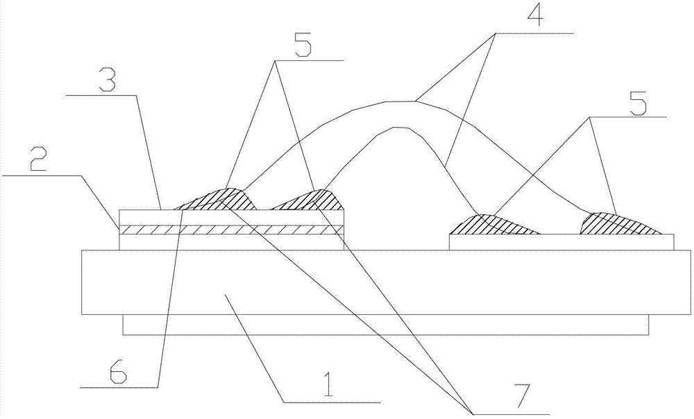
[0035] The height of the glue point 3 formed by the accumulation of the elastic glue at the bottom of the bonding foot 6 and the arc is 1mm, and the shape of the accumulation is not limited.

[0036] The stacking height of glue dots is relatively small, on the one hand, it can reduce the amount of elastic colloid used, on the other hand, it can avoid the impact of excessive accumulation of elastic colloid on other properties of the semiconductor module and affect the use of the semiconductor module.

Embodiment 2

[0038] The rest is the same as that of Example 1, except that the height of the glue point formed by the accumulation of the elastic colloid on the bonding foot and the bottom of the arc is 5mm, and the shape of the accumulation is not limited.

[0039] The stacking height of the glue point is relatively high, which can improve the elastic properties of the elastic colloid, ensure the connection effectiveness of the bonding foot and the bottom of the arc, avoid the breakage of the bonding foot and the starting point of the arc, and ensure the effectiveness of the semiconductor module. The service life of the semiconductor module is reduced, and the cost of use is reduced.

Embodiment 3

[0041] The rest is the same as that of Example 1, except that the height of the glue dot formed by the accumulation of the elastic colloid on the bonding foot and the bottom of the arc is 3 mm, and the shape of the accumulation is not limited.

[0042] The stacking height of the glue point is relatively high, which can improve the elastic properties of the elastic colloid, ensure the effectiveness of the connection between the bonding pin and the bottom of the arc, avoid breakage, ensure the effectiveness of the semiconductor module, improve the service life of the semiconductor module, and reduce the use of cost.


PUM


Abstract

The invention discloses a semiconductor module structure and a connecting and fixing method for bonding wires therein; elastic colloids are arranged in bonding points of chips, DBC substrates and the bonding wires, and are stacked on bonding pins and the bottoms of arc lines to form glue dots. In the working process of the module, the periodical vibration of the arc lines of the bonding wires can be effectively reduced, even eliminated, so that the rupture condition in the bonding pins of the bonding wires and the starting points of the arc lines is avoided, the reliability of the module is guaranteed, and the service life of the module is prolonged.

Description

technical field [0001] The invention belongs to the technical field of power semiconductor module manufacturing, and in particular relates to a semiconductor module structure and a method for connecting and fixing bonding wires in the structure. Background technique [0002] The process of bonding wire bonding is essentially that the welding tool of the bonding machine pulls the bonding wire. Under the control of the ultrasonic energy generated by the equipment, the welding tool separates the electrode surface of the chip, the metal coating on the surface of the copper-clad layer of the DBC substrate, and the The atoms on the surface of the bonding wire are activated to complete the bonding of the chip and the DBC substrate with the bonding wire to realize the circuit connection of the chip. [0003] Aluminum wire bonding is a commonly used chip electrical connection method for power semiconductor module packaging. Aluminum wire bonding has the advantages of small bonding p...

Claims


Application Information

Patent Timeline
Patent Type & Authority Patents(China)
IPC IPC(8): H01L23/498H01L21/60
CPCH01L2224/85H01L2924/00014H01L24/85H01L2224/32225H01L2224/48091H01L2224/48227H01L2224/73265H01L2224/85205H01L2224/8592H01L2924/00H01L2924/00012
Inventor 王豹子
Owner XIAN YONGDIAN ELECTRIC
Learn More