Structure of light-emitting diode structure for improving electrostatic protection and manufacturing method of same

A technology for light-emitting diodes and electrostatic protection, which is applied to circuits, electrical components, and electric solid-state devices. The effect of electrostatic protection

Inactive Publication Date: 2013-02-27
JIANGSU XINGUANGLIAN TECH
View PDF4 Cites 2 Cited by
  • Summary
  • Abstract
  • Description
  • Claims
  • Application Information

AI Technical Summary

Problems solved by technology

Because the human body's perception voltage of electrostatic discharge is about 3KV, and many electronic components will be damaged at hundreds of volts or even tens of volts, usually there is no obvious limit for electronic devices to be damaged by ESD, after the components are installed on the PCB board After re-testing, there were many problems, and the analysis was quite difficult.
Especially for potential damage, it is difficult to measure significant changes in its performance even with precision instruments, so many electronic engineers and designers suspect the hazards of ESD, but experiments in recent years have confirmed that this potential damage after a certain period of time, electronic products Significant drop in reliability

Method used


Image

  • Structure of light-emitting diode structure for improving electrostatic protection and manufacturing method of same
  • Structure of light-emitting diode structure for improving electrostatic protection and manufacturing method of same
  • Structure of light-emitting diode structure for improving electrostatic protection and manufacturing method of same

Examples


Embodiment Construction

[0038] The present invention will be further described below in conjunction with specific drawings.

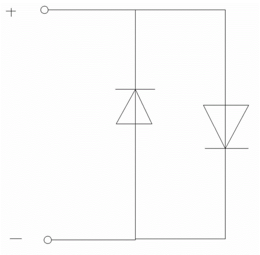
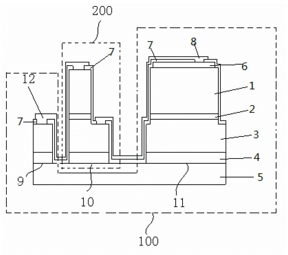
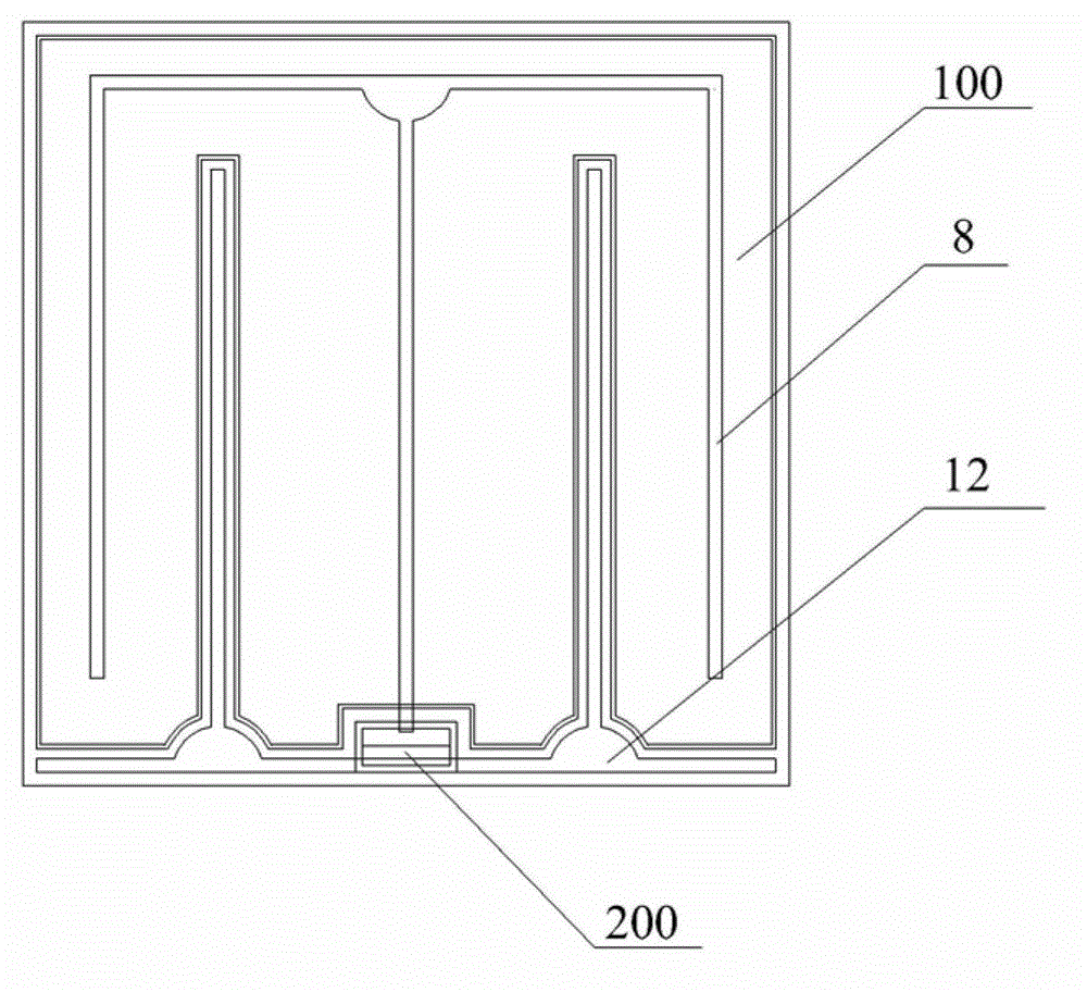
[0039] Such as Figure 2~Figure 13 Shown: the present invention includes a P-type semiconductor layer 1, an active layer 2, an N-type semiconductor layer 3, a buffer layer 4, a substrate 5, a transparent conductive layer 6, a passivation layer 7, a first electrode 8, and a first island-shaped Structure 9 , second island structure 10 , third island structure 11 , second electrode 12 , primary diode 100 , secondary diode 200 .

[0040] Such as figure 2 As shown, the present invention includes a substrate 5, on which a buffer layer 4 and an N-type semiconductor layer 3 are sequentially arranged, the buffer layer 4 covers the substrate 5, and the N-type semiconductor layer 3 covers the buffer layer 4, and, The N-type semiconductor layer 3 and the buffer layer 4 are divided into a first island structure 9, a second island structure 10 and a third island structure 11; in the seco...


PUM


Abstract

The invention relates to a structure of a light-emitting diode structure for improving electrostatic protection, wherein the structure comprises a substrate, a first electrode and a second electrode; a buffer layer and an N-type semiconductor layer are arranged on the substrate in turns; the N-type semiconductor layer and the buffer layer are divided into a first island-shaped structure, a second island-shaped structure and a third island-shaped structure; a source layer and a P-type semiconductor layer are arranged on the second island-shaped structure and the third island-shaped structure in turns; a transparent conductive layer is arranged on the P-type semiconductor layer on the third island-shaped structure; the first island-shaped structure, the P-type semiconductor layer on the second island-shaped structure and the transparent conductive layer are respectively provided with a passivation layer; the first electrode penetrates through the passivation layer to connect with the transparent conductive layer and the N-type semiconductor layer on the second island-shaped structure; and the second electrode penetrates through the passivation layer to connect with the N-type semiconductor layer on the first island-shaped structure and the P-type semiconductor layer on the second island-shaped structure. According to the invention, the electrostatic protection is effectively improved, the damage caused by static electricity is decreased, and the service life of an LED (light-emitting diode) chip is prolonged.

Description

technical field [0001] The invention relates to an LED chip structure, in particular to a structure and a manufacturing method of a light-emitting diode for improving electrostatic protection, and belongs to the technical field of LED chips. Background technique [0002] Electrostatics was established on the basis of Coulomb's law in the 18th century to study the laws of static charges and magnetic fields. It is an important part of electromagnetism in physics. [0003] Static electricity exists everywhere in our daily life, but in the 1940s and 1950s, there were few static electricity problems in the semiconductor industry, because at that time there were transistors and diodes, and the static electricity generated was not as common as it is now. In the 1960s, with the emergence of MOS devices that are very sensitive to static electricity, the problem of static electricity has gradually attracted people's attention. In the 1970s and 1990s, with the increasing density of in...

Claims


Application Information

Patent Timeline
Patent Type & Authority Applications(China)
IPC IPC(8): H01L27/15H01L33/20H01L33/36H01L33/00
Inventor 张淋杜高云邓群雄
Owner JIANGSU XINGUANGLIAN TECH
Why Eureka
Try Eureka