Semiconductor device and manufacturing method thereof

A semiconductor and device technology, applied in the semiconductor device with shallow trench isolation structure and its manufacturing field, can solve the problem that the insulating layer is not removed, and achieve the effects of eliminating dish defects, increasing deposition rate, and reducing differences

Active Publication Date: 2013-03-06
SEMICONDUCTOR MANUFACTURING INTERNATIONAL (BEIJING) CORP
View PDF4 Cites 5 Cited by
  • Summary
  • Abstract
  • Description
  • Claims
  • Application Information

AI Technical Summary

Problems solved by technology

However, this results in a portion of the deposited insulating laye

Method used


Image

  • Semiconductor device and manufacturing method thereof
  • Semiconductor device and manufacturing method thereof
  • Semiconductor device and manufacturing method thereof

Examples


Embodiment Construction

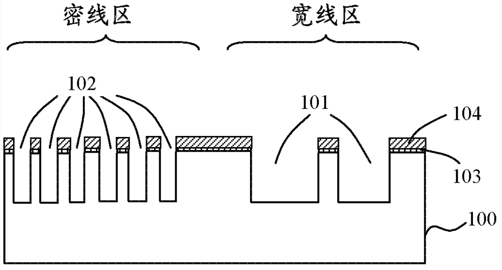
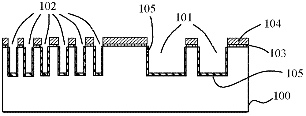
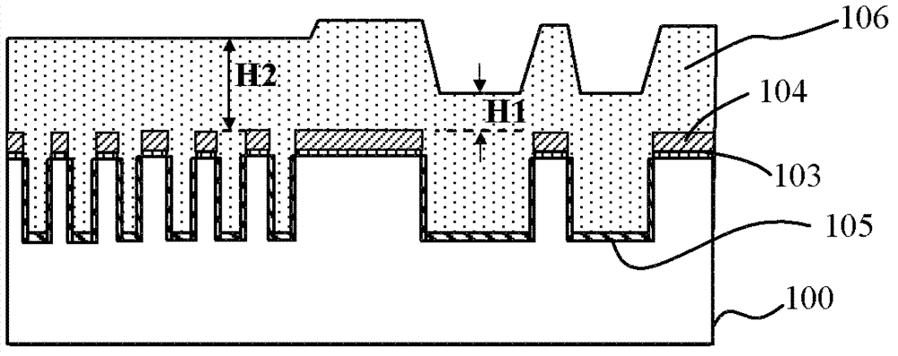
[0040] Various exemplary embodiments of the present invention will now be described in detail with reference to the accompanying drawings. It should be noted that the relative arrangements of components and steps, numerical expressions and numerical values ​​set forth in these embodiments do not limit the scope of the present invention unless specifically stated otherwise.

[0041] At the same time, it should be understood that, for the convenience of description, the sizes of the various parts shown in the drawings are not drawn according to the actual proportional relationship.

[0042] The following description of at least one exemplary embodiment is merely illustrative in nature and in no way taken as limiting the invention, its application or uses.

[0043] Techniques, methods and devices known to those of ordinary skill in the relevant art may not be discussed in detail, but where appropriate, such techniques, methods and devices should be considered part of the Authoriz...


PUM

PropertyMeasurementUnit
Thicknessaaaaaaaaaa
Thicknessaaaaaaaaaa

Abstract

An embodiment of the invention discloses a semiconductor device and a manufacturing method thereof. The manufacturing method includes forming a nitride layer, trenches of a thin line region and trenches of a thick line region are formed on a substrate; forming a first insulation layer on the bottoms and side walls of the formed trenches of the thin line region and the trenches of the thick line region; removing part of or total of the first insulation layer on the trenches of the thin line region only; depositing a second insulating layer to fill the trenches of the thin line region and the trenches of the thick line region; according to chemical mechanical planarization technology, planarizing the second insulation layer outside trenches of the thin line region and the trenches of the thick line region by utilizing the nitride layer as a barrier layer. Since the part of or the total of the first insulation layer at the bottom of the thin trench region is removed in the manufacturing method, deposition rate of the second insulation layer in the thin trench region is increased, difference of the second insulation layer deposited in the thin line region and the thick line region is reduced, and dishing defect caused in the chemical mechanical planarization process is relived or eliminated.

Description

technical field [0001] The present disclosure relates to the field of semiconductor device manufacturing, in particular to a semiconductor device with a shallow trench isolation structure and a manufacturing method thereof. Background technique [0002] As the integration level of semiconductor devices continues to increase, isolation techniques for electrically isolating adjacent devices become more and more important. The shallow trench isolation process is an isolation technology widely used in the manufacture of highly integrated semiconductor devices. [0003] The shallow trench isolation process realizes effective isolation of the active region by forming an isolation trench defining an active region on a semiconductor substrate and filling the isolation trench with an insulating material. Generally, some areas in semiconductor devices have higher density of active areas, and the width of trenches for isolation of active areas is smaller. This area is called "dense li...

Claims


Application Information

Patent Timeline
IPC IPC(8): H01L21/762
CPCH01L29/06H01L21/302H01L21/76229
Inventor 邵群洪中山
Owner SEMICONDUCTOR MANUFACTURING INTERNATIONAL (BEIJING) CORP
Why Eureka
Try Eureka