Method for preventing optical feedback of semiconductor laser processing machine

A laser processing machine and laser processing technology, applied in the direction of semiconductor laser devices, laser devices, laser welding equipment, etc., can solve problems such as damage, shortened life, and decreased output power of lasers, so as to reduce damage, prevent life reduction, and output light Effect of Power Density Improvement

Inactive Publication Date: 2013-03-13
CHANGCHUN INST OF OPTICS FINE MECHANICS & PHYSICS CHINESE ACAD OF SCI
View PDF8 Cites 7 Cited by
  • Summary
  • Abstract
  • Description
  • Claims
  • Application Information

AI Technical Summary

Problems solved by technology

However, when the laser processing is performed on the surface of a metal workpiece at such a high power, part of the reflected light on the surface of the workpiece will return to the cavity of the semiconductor laser along the original optical path, which will cause damage to the inside of the semiconductor laser and its cavity film, and then make the laser. Decreased output power and shortened life
Since the current semiconductor laser processing machines use polarization beam combining and wavelength beam combining, and the reflected beam has the same wavelength as the light emitted by the laser, and returns along the original optical path, it is difficult to pass through the optical path in the optical system. The traditional method of processing its reflected light

Method used


Image

  • Method for preventing optical feedback of semiconductor laser processing machine

Examples


Embodiment Construction
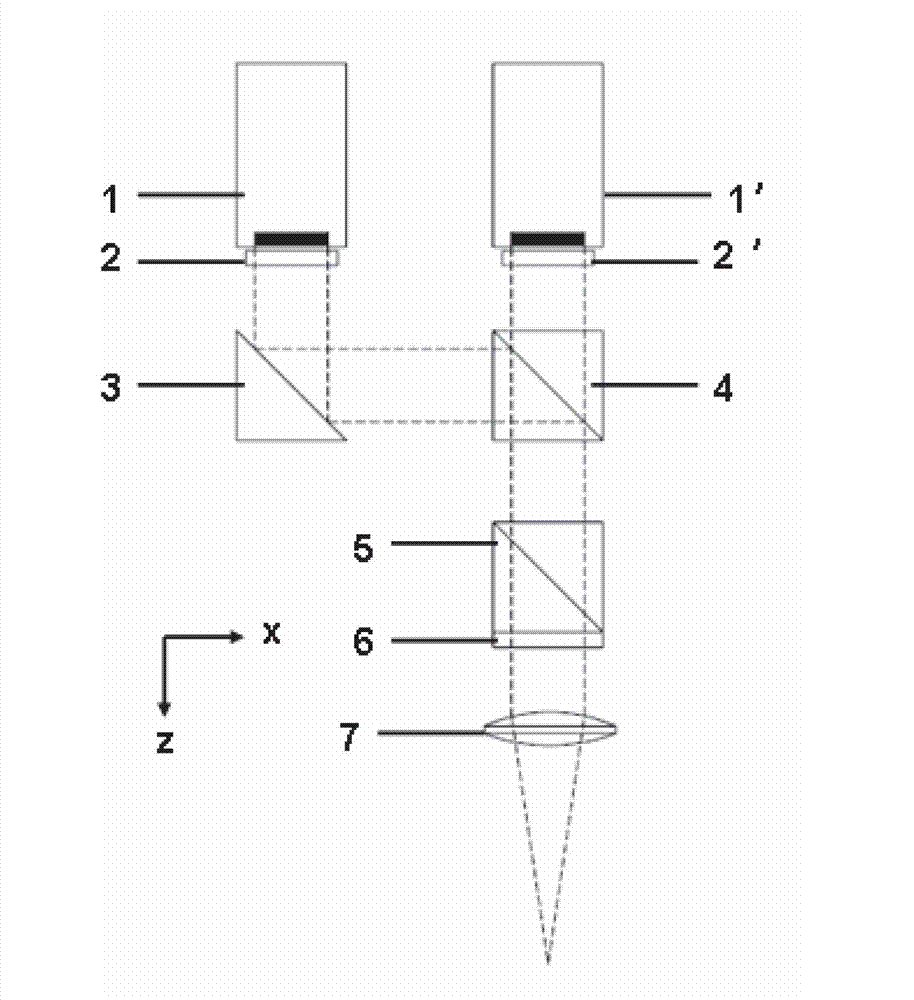
[0024] The inventive idea of ​​the present invention is: a method for preventing optical feedback of a semiconductor laser processing machine. The stack respectively emits a wavelength of λ 1 and lambda 2 P or S polarization state of the laser beam. The method for preventing optical feedback of semiconductor laser processing machine of the present invention is to utilize:

[0025] A reflective prism that is set at 45° to the optical path is arranged before one of the semiconductor laser stacks; the other semiconductor laser is set in turn before the stack, and a wavelength beam combining prism and a polarization beam splitter are set at 45° with the optical path, and A quarter-wave plate and a focusing mirror set perpendicular to the optical path;

[0026] The light emitted by one of the semiconductor laser stacks passes through the reflective prism, and the propagation direction is rotated by 90°; the light emitted by the other semiconductor laser stack is directly inciden...


PUM

PropertyMeasurementUnit
wavelengthaaaaaaaaaa
reflectanceaaaaaaaaaa

Abstract

The invention relates to a method for preventing optical feedback of a semiconductor laser processing machine. The method comprises the following steps of: arranging a reflecting prism arranged at an angle of 45 degrees with an optical path in front of aone semiconductor laser stack array; respectively and sequentially arranging a wavelength beam closing prism and a polarizing prism arranged at an angle of 45 degrees with the optical path as well as a one-fourth wave plate and a focusing mirror which are arranged perpendicular to the optical path in front of the other semiconductor laser stack array; rotating the propagating direction of light emitted by the semiconductor laser stack array passing through the reflecting prism by 90 degrees; enabling light emitted by another semiconductor laser stack array to directly irradiate the wavelength beam closing prism and closing beams of two beams of laser through the wavelength beam closing prism; propagating the closed light beams along the laser transmitting direction of the semiconductor laser stack array; and enabling the closed light beams to pass through the polarizing prism and the one-fourth wave plate and focusing the closed beams by the focusing mirror. According to the method disclosed by the invention, the damage to the inside and a cavity surface film of the laser can be effectively reduced and the service life of the laser is prolonged.

Description

technical field [0001] The invention relates to an application method of a semiconductor laser processing machine, in particular to a method for preventing optical feedback of the semiconductor laser processing machine. Background technique [0002] Due to the continuous improvement and improvement of semiconductor lasers in terms of output power, electro-optical conversion efficiency, reliability and cost, the use of high-power semiconductor lasers for material processing has become an international hotspot. As an advanced manufacturing technology, high-power semiconductor laser processing technology has great advantages in improving product productivity, processing automation, environmental pollution and reducing cost consumption. In laser processing applications, the optical power of a single semiconductor laser stack can no longer meet the actual needs. In order to increase the output power of high-power semiconductor lasers, it is required to combine the light emitted b...

Claims


Application Information

Patent Timeline
Patent Type & Authority Applications(China)
IPC IPC(8): B23K26/00B23K26/06H01S5/40B23K26/064
Inventor 朱洪波郝明明秦莉王立军
Owner CHANGCHUN INST OF OPTICS FINE MECHANICS & PHYSICS CHINESE ACAD OF SCI
Why Eureka
Try Eureka