
Method for programming of multi-bit semiconductor memory

A memory and semiconductor technology, applied in static memory, read-only memory, information storage, etc., can solve the problems of large distribution range of threshold voltage of memory cells, increase memory programming time, low pulse amplitude, etc., and reduce the distribution range of threshold voltage. , The effect of reducing the threshold voltage distribution range and improving the reset speed

Inactive Publication Date: 2013-03-13
INST OF MICROELECTRONICS CHINESE ACAD OF SCI
View PDF2 Cites 0 Cited by
  • Summary
  • Abstract
  • Description
  • Claims
  • Application Information

AI Technical Summary

Problems solved by technology

To make the threshold voltages of all memory devices distributed in a narrow range after programming, the pulse amplitude applied during programming should be low, so that after each programming, the threshold voltage of memory devices increases by a small amount, but in this way It will significantly increase the number of programming times for a single cell, thereby greatly increasing the memory programming time; if you want to speed up the memory programming speed and reduce the programming time, you need to apply a larger pulse during programming, so that after each programming, the threshold voltage of the memory cell The increase is relatively large, but this will lead to a large distribution range of the threshold voltage of the memory cell after programming

Method used


Image

  • Method for programming of multi-bit semiconductor memory
  • Method for programming of multi-bit semiconductor memory
  • Method for programming of multi-bit semiconductor memory

Examples


Embodiment Construction

[0029]In order to make the object, technical solution and advantages of the present invention clearer, the present invention will be described in further detail below in conjunction with specific embodiments and with reference to the accompanying drawings.

[0030] In the method for programming a multi-bit semiconductor memory provided by the present invention, by applying a larger programming voltage in the first round of programming operation, the threshold voltages of all memory cells are programmed to one near the specified threshold voltage in a shorter period of time. within a larger range, and then by applying a smaller programming voltage in the second round of soft programming operations, the threshold voltages of all memory cells are programmed to a smaller range around the specified voltage; through the above two steps, effective The programming time and programming accuracy of the multi-bit semiconductor memory are greatly improved.

[0031] Such as Figure 5 as s...


PUM


Abstract

The invention discloses a method for programming of a multi-bit semiconductor memory, and relates to the technical field of semiconductor memories. The method comprises the following steps: performing reset operation of all memory cells in the multi-bit semiconductor memory; performing a first turn of programming operation, that is programming threshold voltages of all the memory cells in the multi-bit semiconductor memory to be in a voltage range lower by 0.5 volt than the specified threshold voltages of the memory cells; and performing a second turn of programming operation, that is programming the threshold voltages of all the memory cells in the multi-bit semiconductor memory to be in a voltage range of + / - 0.05 volt of the specified threshold voltages of the memory cells. The invention effectively solves the contradiction between memory reset speed and reset precision, on one hand, improves the reset speed of the memory, on the other hand, greatly reduces the distribution scope of the memory cell threshold voltage after reset.

Description

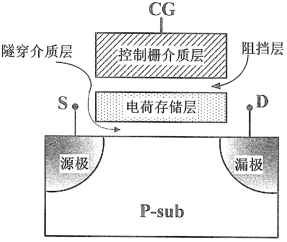
technical field [0001] The invention relates to the technical field of semiconductor memory, in particular to a method for programming a multi-bit semiconductor memory. Background technique [0002] At present, the development of memory technology has become an important driving force for the advancement of integrated circuit design and manufacturing, and occupies a very important position in the field of microelectronics. [0003] Such as figure 1 as shown, figure 1 It is a very important type of semiconductor memory - a schematic diagram of the stack gate non-volatile memory structure. The memory structure includes a silicon substrate (P-sub), n-type heavily doped source region (S) and drain region (D) on the silicon substrate, and a tunnel covering the carrier channel between the source and drain regions. A dielectric layer, a charge storage layer covering the tunnel dielectric layer, a barrier layer covering the charge trapping layer, and a control gate dielectric lay...

Claims


Application Information

Patent Timeline
Patent Type & Authority Applications(China)
IPC IPC(8): G11C16/10
Inventor 刘明姜丹丹霍宗亮张满红刘璟谢常青
Owner INST OF MICROELECTRONICS CHINESE ACAD OF SCI
Learn More