A coupling package structure of optical waveguide chip and pd array

A waveguide chip and optical waveguide technology, applied in the field of communications, can solve problems such as affecting the normal operation of modules, decreasing coupling efficiency, and substandard products, and achieving the effects of solving mechanical reliability problems, ensuring integrity, and reducing the amount of variation

Active Publication Date: 2014-10-01
GUANGXUN SCI & TECH WUHAN
View PDF9 Cites 1 Cited by
  • Summary
  • Abstract
  • Description
  • Claims
  • Application Information

AI Technical Summary

Problems solved by technology

The device can work normally at room temperature. If the optoelectronic device is applied in a wide temperature range, the relative position of the waveguide chip and the PD may shift, which will greatly reduce the coupling efficiency and affect the subsequent circuit. The output result of the signal, more serious may lead to product failure
[0005] In the article "Packaging for a 40 channel Parallel Optical Interconnection Module with An Over 25 Gbit / s Throughput", the author proposes a waveguide chip and PD array coupling packaging structure, this structure is in the temperature range of -5 to 75 degrees, Due to the different expansion coefficients of each material, the relative position of the waveguide chip and the PD array has a maximum deviation of micron level, and the position deviation will directly lead to a decrease in coupling efficiency, and even affect the normal operation of the entire module

Method used


Image

  • A coupling package structure of optical waveguide chip and pd array
  • A coupling package structure of optical waveguide chip and pd array
  • A coupling package structure of optical waveguide chip and pd array

Examples


Embodiment Construction

[0050] The present invention is further described in conjunction with the accompanying drawings.

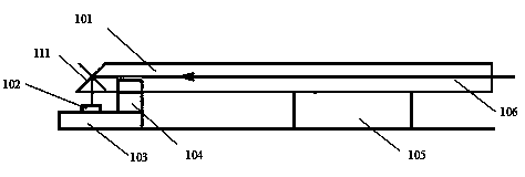
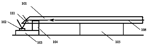
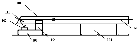
[0051] The present invention provides an optical waveguide chip and PD array coupling packaging structure such as Figure 5As shown, it includes a waveguide chip 101 , a PD array 102 , a waveguide support frame 105 , a substrate 103 , and a U-shaped spacer 104 . The substrate 103 and the waveguide support frame 105 are respectively arranged on the bottom plate 107, and the waveguide chip 101 is fixed on the waveguide support frame 105. The output end surface of the waveguide chip 101 has a certain inclination angle, and its end surface is coated with a total reflection film, so that the The light totally reflected by the inclined surface is deflected by a certain angle and obliquely strikes the photosensitive surface of the PD array 102 . Substrate 103 is provided with such as Figure 6a The first marking line surface 108 and the second marking line surface 109 are shown. The ...


PUM


Abstract

The invention discloses an optical waveguide chip and PD (photodiode) array coupling packaging structure. The optical waveguide chip and PD array coupling packaging structure comprises a soleplate, a waveguide supporting rack, a waveguide chip and a substrate, wherein a third sign line surface is arranged on the back surface of the substrate of the waveguide chip; a first sign line surface and a second sign line surface are arranged on the substrate respectively; the PD array with an upward photosensitive surface is adhered to the first sign line surface; a U-shaped spacer with an upward opening is adhered to the second sign line surface; the groove width of the U-shaped spacer is equal to the width of the waveguide chip; and the waveguide chip, of which the third sign line surface and the second sign line surface have corresponding widths, penetrates through a U-shaped groove of the U-shaped spacer and is positioned over the PD array. The optical waveguide chip and PD array coupling packaging structure can control axial positions, so that passive alignment of the optical waveguide chip and the PD array can be achieved.

Description

technical field [0001] The invention relates to an optical waveguide chip and a PD (Photo-Diode photodiode) array coupling packaging structure, and the invention belongs to the communication field. Background technique [0002] With the development of high-speed information technology, the development of integrated optical devices has become an inevitable trend in the interlaced development of various fields such as optical communication, optical computing, and optical sensing in the future. As the information capacity continues to increase, its transmission rate also continues to increase, so the requirements for the integration and stability of the devices in the system are also continuously improved. The development of high-speed optical communication is becoming more and more rapid. One of the most important features is the improvement of device integration, and optoelectronic integration technology will be more widely used in the system. PM-QPSK modulation is used in 1...

Claims


Application Information

Patent Timeline
Patent Type & Authority Patents(China)
IPC IPC(8): G02B6/42
Inventor 石川梁雪瑞陈征江雄汪灵杰
Owner GUANGXUN SCI & TECH WUHAN
Why Eureka
Try Eureka