
Method for growing InP base InAs quantum well

A quantum well and quantum well layer technology, which is applied in the field of semiconductor materials and device chip preparation, can solve the problems of affecting material quality, material quality degradation, increasing device series resistance and manufacturing cost, etc., to achieve the expansion of luminescent wavelength and the reduction of band gap small effect

Inactive Publication Date: 2013-03-20
INST OF SEMICONDUCTORS - CHINESE ACAD OF SCI
View PDF4 Cites 5 Cited by
  • Summary
  • Abstract
  • Description
  • Claims
  • Application Information

AI Technical Summary

Problems solved by technology

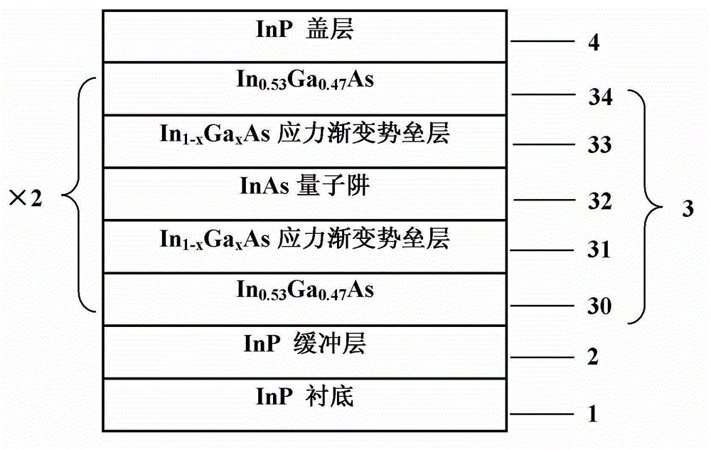
[0004] InP-based InAs / In 0.53 Ga 0.47 There are two problems in the epitaxial growth of As quantum wells: 1. There is a huge lattice mismatch (3.2%) between the InAs quantum wells and the InP substrate, and the InAs quantum well material will produce defects under the condition of large compressive strain , affecting the quality of the material; 2. According to the law of quantum confinement effect, prolonging the luminous wavelength of the InAs quantum well requires increasing the thickness of the InAs layer, but this will cause the aggravation of the material strain, resulting in more defects, resulting in a decline in the quality of the material
However, the pseudo-substrate structure requires epitaxy of a pseudo-substrate material with a large thickness (>3 μm) and a gradual change in lattice constant, which increases the series resistance and manufacturing cost of the device to a certain extent.

Method used


Image

  • Method for growing InP base InAs quantum well
  • Method for growing InP base InAs quantum well
  • Method for growing InP base InAs quantum well

Examples


Embodiment Construction

[0017] In order to make the object, technical solution and advantages of the present invention clearer, the present invention will be described in further detail below in conjunction with specific embodiments and with reference to the accompanying drawings.

[0018] It should be noted that, in the drawings or descriptions of the specification, similar or identical parts all use the same figure numbers. Implementations not shown or described in the accompanying drawings are forms known to those of ordinary skill in the art. Additionally, while illustrations of parameters including particular values ​​may be provided herein, it should be understood that the parameters need not be exactly equal to the corresponding values, but rather may approximate the corresponding values ​​within acceptable error margins or design constraints. In addition, the directional terms mentioned in the following embodiments, such as "upper", "lower", "front", "rear", "left", "right", etc., are only re...


PUM

PropertyMeasurementUnit
Growth thicknessaaaaaaaaaa
Thicknessaaaaaaaaaa
Thicknessaaaaaaaaaa

Abstract

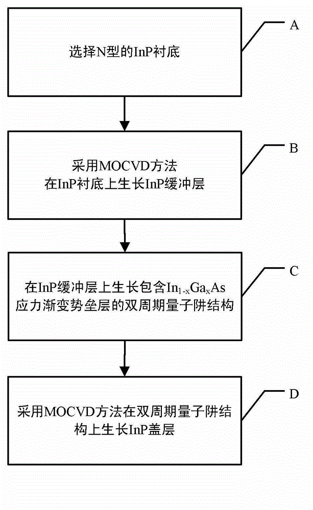
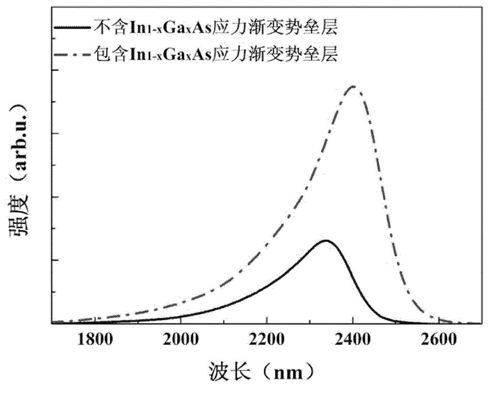
The invention provides a method for growing an InP base InAs quantum well. The method comprise the steps of growing an InP buffering layer on an InP substrate, growing an InAs quantum well structure on the InP buffering layer, and growing an InP cover layer on the InAs quantum well structure, wherein In[1-x]Ga[x]As stress gradation barrier layers are formed on the two sides of the InAs quantum well structure. According to the method, the In[1-x]Ga[x]As stress gradation barrier layers with gradual lattice constant are introduced on the two sides of the InAs quantum well to decelerate compression strain suffered by the InAs quantum well; defect concentrations in materials, which are produced due to the accumulated release of the strain, are reduced; the crystal quality of the InAs quantum well materials is improved; and luminous wavelengths of the InAs quantum well materials are extended.

Description

technical field [0001] The invention belongs to the field of semiconductor material and device chip preparation, in particular to a method for growing an InP-based InAs quantum well. Background technique [0002] Due to the huge potential application advantages in gas detection and biomedicine, InP-based InAs quantum well materials and devices (lasers and detectors, etc.) with a light emission wavelength in the range of 2-3 μm have many advantages such as low cost and mature device technology. [0003] In 1994, InAs was used as the well, In 0.53 Ga 0.47 The InP-based quantum well structure material with As barrier was first applied in 1.7μm quantum well laser. With the development of metal organic compound vapor deposition (MOCVD) epitaxy technology, the application wavelength range of this material system has been expanded. In 2007, 2.33μm InP-based InAs / In 0.53 Ga 0.47 As quantum well laser. [0004] InP-based InAs / In 0.53 Ga 0.47 There are two problems in the epita...

Claims


Application Information

Patent Timeline
IPC IPC(8): H01L21/205
Inventor 季海铭罗帅杨涛
Owner INST OF SEMICONDUCTORS - CHINESE ACAD OF SCI
Learn More