Structured circuit board and method
A technology of circuit boards and conductive vias, applied in circuits, printed circuits, printed circuits, etc., can solve problems such as signal loss, achieve the effects of reducing separation, reducing manufacturing costs, and reducing crosstalk
- Summary
- Abstract
- Description
- Claims
- Application Information
AI Technical Summary
Problems solved by technology
Method used
Image
Examples
Embodiment Construction
[0026] Note that the views are schematic, not necessarily to scale, and details not necessary for an understanding of the invention may have been omitted. The terms "upward", "downward", "below", "above" etc. relate to the embodiment as oriented in the views. In addition, elements that are at least substantially the same or perform at least substantially the same function are denoted by the same reference numerals.
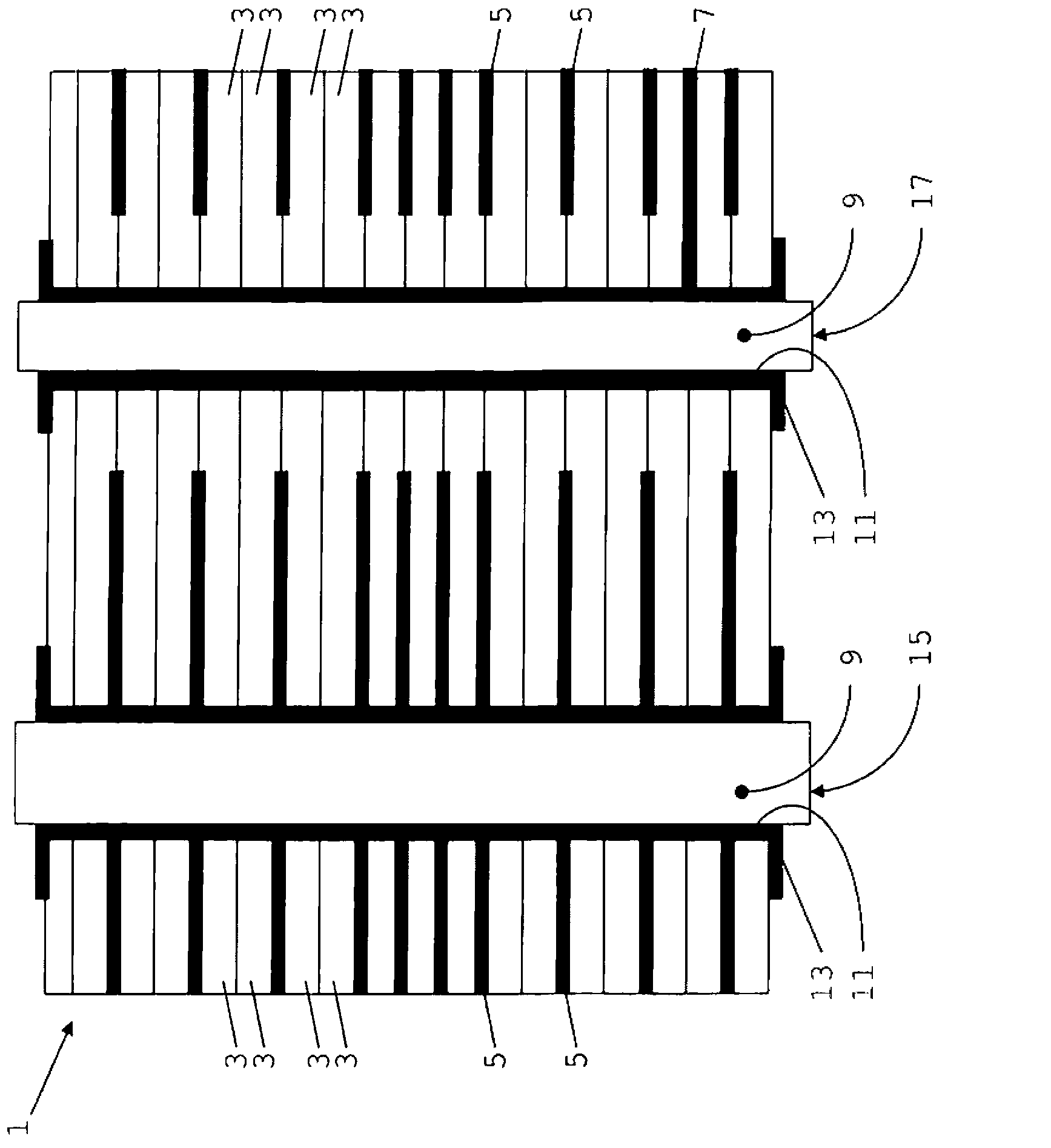
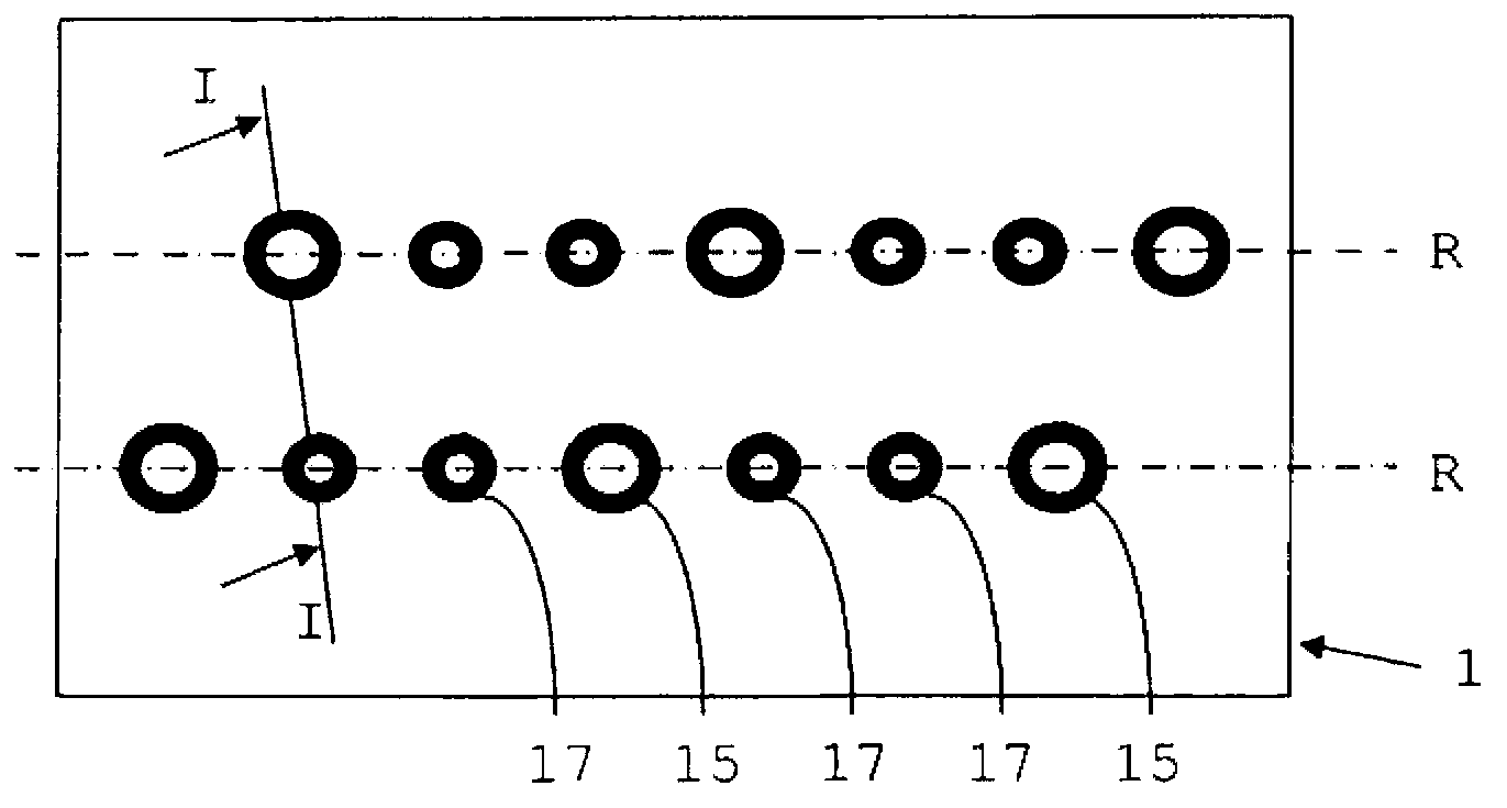
[0027] figure 1 show figure 2 A cross section of a part of a prior art multilayer circuit board 1 shown in top view in . figure 2 yes figure 1 A top view of circuit board 1, indicating the figure 1 section. The circuit board 1 includes a plurality of insulating layers 3 separated by a plurality of ground layers 5 and a plurality of layers including signal traces 7 ( figure 1 Only one signal trace is shown in 7). The insulating layers may be substantially identical or may differ from each other in one or more respects, in particular in size and / or in one o...
PUM
 Abstract
Description
Claims
Application Information


