

Varifocal photoetching objective lens system
A lithography objective lens and zoom technology, applied in the field of optics, can solve the problem that the same lithography objective lens cannot expose mask exposure patterns of different scales and sizes, etc., and achieves short optical total length, small aperture, and reduces processing difficulty. and the effect of manufacturing costs
- Summary
- Abstract
- Description
- Claims
- Application Information
AI Technical Summary
Problems solved by technology
Method used
Image

Examples
Embodiment 1
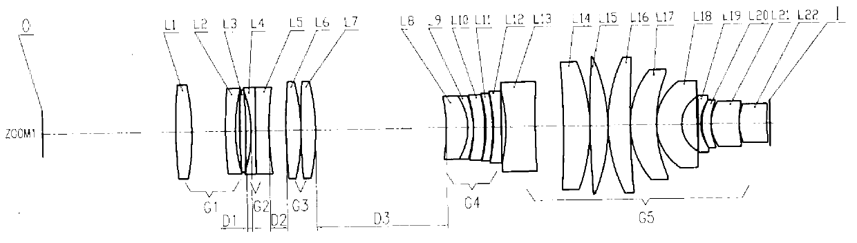
[0041] Embodiment 1: as figure 1 As shown, the present invention provides a kind of refraction zoom lithography objective lens system working at a wavelength of 410nm according to the structure of zoom1, which is used to image the pattern of the object plane O on the image plane I, which is composed of 22 optical lenses, From the object plane to the image plane, the lenses are marked as L1~L22. The 22 optical lenses are divided into G1~G5 groups according to their power and their functions in the system of the present invention. The distribution of power is from the object plane to the image. The planes are positive-negative-positive-negative-positive in turn, the distance from the object plane to the image plane is 805mm, the largest lens in the system has a full aperture of less than 153mm, the F number of the image side is 2, the numerical aperture of the image side is 0.2, and the magnification is 0.25. The size is 14.8mm.
[0042] The specific structure of the zoom litho...
Embodiment 2
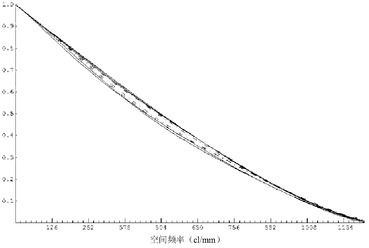
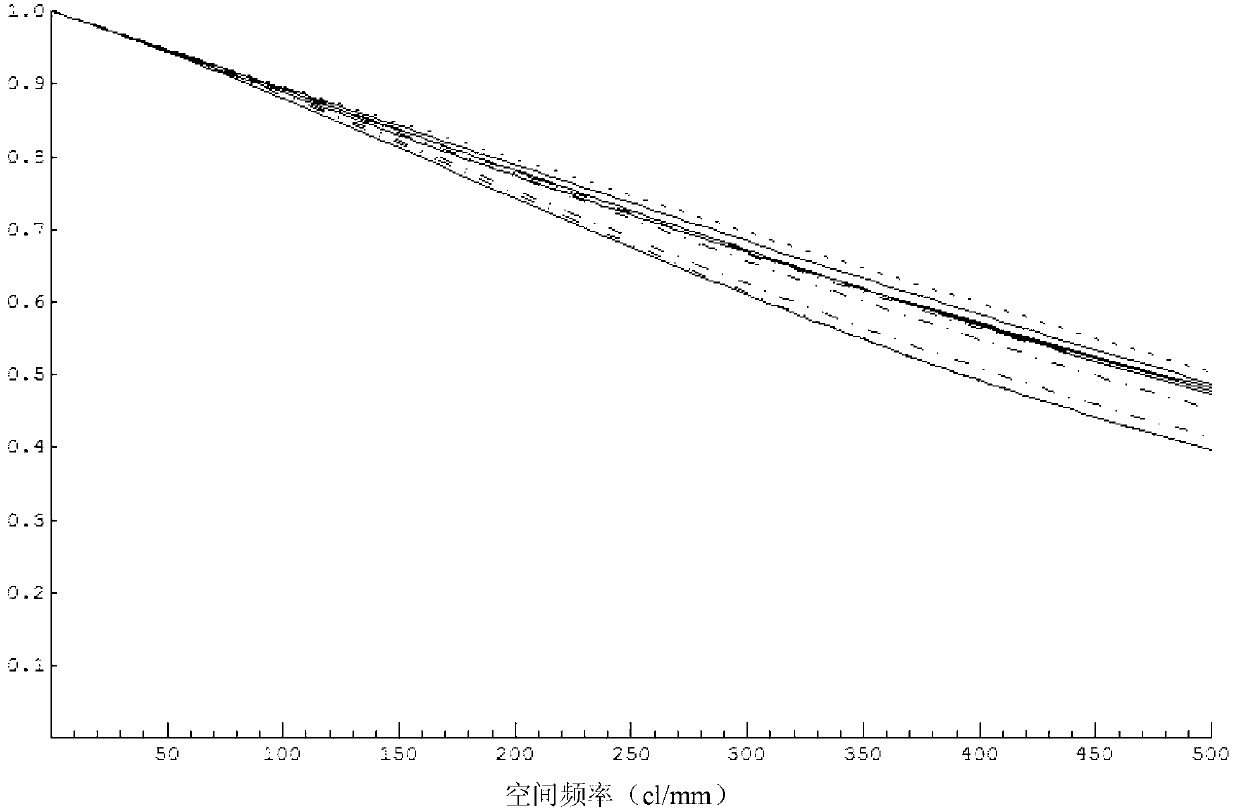
[0059] Such as Figure 5 As shown, the structure diagram of the present invention at the zoom position zoom2, such as Figure 6 As shown, the transfer function graph of the optical system at the zoom position zoom2, such as Figure 7 As shown, the graph of the transfer function when the defocus is 1μm, such as Figure 8 As shown, field curvature and distortion graphs.
Embodiment 3
[0061] Such as Figure 9 As shown, the structure diagram of the present invention at the zoom position zoom3, such as Figure 10 As shown, the transfer function graph of this optical system, such as Figure 11 As shown, the graph of the transfer function when the defocus is 1μm, such as Figure 12 As shown, field curvature and distortion graphs.
PUM
 Abstract
Description
Claims
Application Information