

Method for improving stability of alignment precision of high-transparency mask plate
A technology with high light transmittance and overlay accuracy, applied in the field of semiconductor manufacturing, can solve the problems of affecting the production efficiency of lithography process, offset of registration accuracy, and reduction of wafer yield, so as to improve yield and process production. Efficiency, reducing the degree of thermal expansion of the lens, and maintaining stable overlay accuracy
- Summary
- Abstract
- Description
- Claims
- Application Information
AI Technical Summary
Problems solved by technology
Method used
Image

Examples
Embodiment Construction
[0019] The method for improving the stability of the overlay accuracy of the high-transmittance mask plate proposed by the present invention will be further described in detail below in conjunction with specific embodiments. Advantages and features of the present invention will be apparent from the following description and claims.
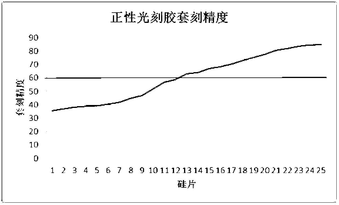
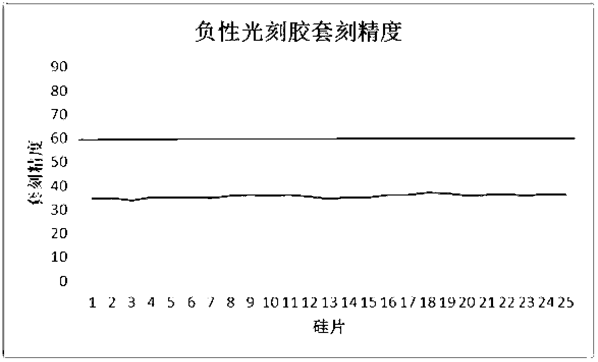
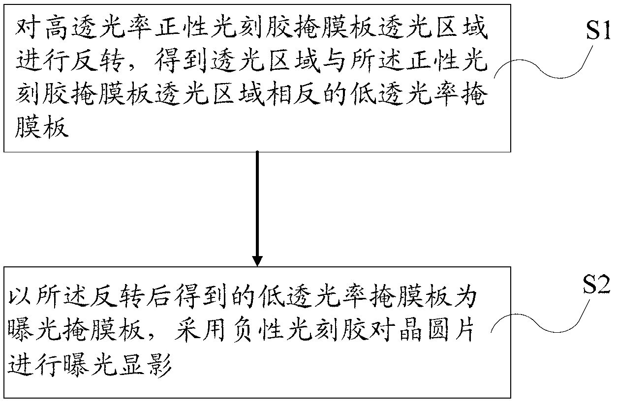
[0020] The core idea of the present invention is to provide a method for improving the stability of the overlay accuracy of a high-transmittance mask plate. In this method, the light-transmitting area of the high-transmittance positive photoresist mask plate is first reversed to obtain The low light transmittance mask whose light transmission area is opposite to the light transmission area of the positive photoresist mask, and then use the low light transmittance mask obtained after the inversion as the exposure mask, using Negative photoresist exposes and develops the wafer, which effectively reduces the heat energy of the lens during the e...
PUM
 Abstract
Description
Claims
Application Information